Checkpoint 4: Caches and
DDR2
CS 150, UC Berkeley, Fall 2011
0 Introduction & Motivation
The first three checkpoints were concerned with creating a base system consisting of a MIPS CPU and a serial communication interface. At this stage, the CPU is able to run C code and interact over serial - no small feat for a few weeks of work. However, there is still one significant limitation the design will need to overcome to allow for more complex programs and a graphics engine: Memory capacity.
Through checkpoint 3, the instruction and data memory was entirely comprised of Block RAMs, of which the Virtex-5 XC5VLX110T has approximately 5 MB. The over-arching purpose of this checkpoint is to move to a new memory architecture utilizing high capacity DDR2 for storage.
Switching to DDR2 has several implications for your design. Recall from lecture that in general, as you switch to higher capacity storage mediums, access time grows by comparable orders of magnitude. In this case, we are moving from one-cycle access to the on-die block RAMs to multi-cycle access to the SODIMM (small outline dual-inline memory module) mounted on the back of the development boards.
To mitigate the performance penalty from the slow memory access, you will add data and instruction caches to your design. Additionally, you will need to add logic in your CPU to enable stalling when one of the caches misses.
This checkpoint will be divided into two parts: Cache
implementation and stall implementation.
Table of Contents
2.4 MIG (Memory Interface Generator) Details
7.4 Instruction Cache Simulation
8 Generating Block RAMs in Coregen
1 Overview
This checkpoint adds caches, clock-crossing FIFOs and Xilinx’s DDR2 controller to the block diagram:
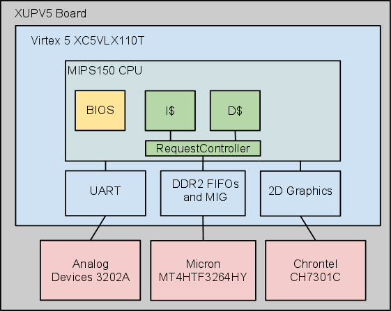
As can be seen in the diagram, the interface to this SODIMM will leverage the work done by Xilinx to develop the MIG (memory interface generator) tool. This tool is run through Coregen and supports a handful of DRAM types and timings. The staff have provided the generated modules, a module connecting the clock-crossing FIFOs to the DDR2 controller, and a module that interleaves requests when the two caches have access collisions.
2 New Modules
The staff have provided a set of skeleton modules that implement DDR2 access and should help organize your cache. The modules provided are as follows:
2.1 Cache.v
This is where you should implement the cache. As will be described in further detail in Section 3, you will have the freedom to choose the capacity, block size, etc. of cache as you see fit. However, we have given you some specific suggestions for what to start with in Section 3.
You will need to generate and instantiate block RAM(s) for your cache, design the logic for the finite state machine that will govern the caches behavior, and interface with the clock-crossing-FIFOs to read and write from DDR2. The skeleton files provide the following interface, which should not be changed:
|
Name |
Width |
Direction |
Description |
|
clk |
1 |
input |
Same clock as your CPU (cpu_clk_g) |
|
rst |
1 |
input |
Same reset as your CPU receives |
|
addr |
32 |
input |
Byte-address from CPU for load or store operation |
|
din |
32 |
input |
Data in for writes |
|
we |
4 |
input |
Byte-mask write enable signal (same as in Block RAMs) |
|
re |
1 |
input |
Read enable signal |
|
rdf_valid |
1 |
input |
From read FIFO, indicates that rdf_dout is valid |
|
rdf_dout |
128 |
input |
Half of a block of data from the read FIFO |
|
af_full |
1 |
input |
Indicates the address and command FIFO are full |
|
wdf_full |
1 |
input |
Indicates the write data FIFO is full |
|
stall |
1 |
output |
Indicates the CPU should stall |
|
dout |
32 |
output |
Data output to CPU at completion of read operation |
|
rdf_rd_en |
1 |
output |
Set high when waiting to read the data FIFO |
|
af_cmd_din |
3 |
output |
DDR2 command (000 for write, 001 for read) |
|
af_addr_din |
31 |
output |
DDR2 address |
|
af_wr_en |
1 |
output |
Write to the address FIFO (if !af_full) |
|
wdf_din |
128 |
output |
Data to write to the write data FIFO on wdf_wr_en_assertion |
|
wdf_mask_din |
16 |
output |
Activate-low byte-mask for the DDR2 |
|
wdf_wr_en |
1 |
output |
Write to the data FIFO (if !wdf_full) |
Your cache will need to handle capacity, conflict and
compulsory misses. The FIFO signals provide the following
means of reading and writing to the DDR2:
To execute a write
- Supply a 31-bit address to af_addr_din, of which the low 25-bits matter, while the upper 6 should be zero.
- Set af_cmd_din to 3'b000.
- Supply 128-bits worth of data to wdf_din.
- Supply 16-bits worth of byte mask to wdf_mask_din, remember this signal is active low.
- Assert wdf_wr_en and af_wr_en when !af_full && !wdf_full
- Supply the next 128 bits of data and assert wdf_wr_en when !wdf_full
To execute a read
- Supply a 31-bit address to af_addr_din, of which the low 25-bits matter, while the upper 6 should be zero.
- Set af_cmd_din to 3'b001
- Assert af_wr_en when !af_full
- Assert rdf_rd_en to indicate waiting for data
- Wait for rdf_data_valid to be asserted and store the first half of the block
- Wait for rdf_data_valid to be asserted again and store the second half of the block, and set rdf_rd_en low again.
2.2 Memory150.v
You will not need to change this module but you will need to understand it in order to implement your cache. This module contains several important pieces of the new memory architecture:
- DDR2 interface: The mig_v3_61 module instantiated here is Xilinx’s generated DDR2 controller for the SODIMM on our boards. The DDR2 module runs at 200 MHz and there are new clock signals coming in from ml505top to accommodate this. The DDR2 controller uses FIFOs (you should review Lectures 11 and 15 if you don’t have a good understanding of FIFOs) to receive commands and return data; these are in turn connected to clock crossing FIFOs to return to the clock domain of cpu_clk_g.
- Clock crossing FIFOs:
- mig_af: This FIFO accepts addresses and commands from the RequestController and sends them to mig_v3_61.
- mig_wdf: This FIFO accepts write data from the RequestController in 128-bit blocks and sends it to mig_v3_61.
- mig_rdf: This FIFO receives data from mig_v3_61 and makes it available to the RequestController.
- RequestController, described in the next section.
- The data and instruction caches.
This module also routes read enable, write mask, address, data in and data out from your CPU to both your instruction and data caches.
2.3 RequestController.v
You will not need to change this module but you will need to understand it in order to implement your cache. This module’s primary purpose is to give each cache the illusion of having exclusive access to the clock-crossing-FIFOs. This is accomplished by asserting af_full and wdf_full to the data cache (which should make the instruction cache stall) when both caches need to read or write from DDR2 - i.e., the instruction cache is given priority over the data cache. Additionally, this module tracks read request ordering and directs data out from the DDR2 to the appropriate cache.
There are a few assumptions about the behavior of the cache that are required for this module to function as intended:
- Your cache must assert rdf_rd_en when waiting for data from the DDR2
- Your cache must only assert af_wr_en and wdf_wr_en when af_full and wdf_full are 0, respectively.
- Your cache must read the data in on the first cycle that it receives rdf_valid high.
In order for your cache module to function with the given interface and skeleton files, it is important that your cache adheres to the read/write procedure described in the Cache.v section as well as the expectations of the RequestController.
2.4 MIG (Memory Interface Generator) Details
(Note: The staff have provided these modules, their instantiations, and the neccessary wiring. This section is for reference during simulation and testing.)
The Memory150 module interfaces with the DDR2 on the board via the MIG modules. The module of most immediate interest is the mig_v3_61 module. This is the highest level MIG module and provides the most easy to use interface to the user. This interface consists of the following system signals (already implemented for you in Memory150):
|
Name |
Width |
Direction |
Description |
|
clk0 |
1 |
input |
Clock signal input for MIG core to run at |
|
clk90 |
1 |
input |
Clock signal input that is clk0 phase shifted by 90 degrees. |
|
clkdiv0 |
1 |
input |
Clock signal input that is half the speed of clk0. |
|
clk200 |
1 |
input |
Clock signal input at 200 MHz used to drive IDELAYCTRL. |
|
locked |
1 |
input |
Indicates that the driving PLL has locked. |
|
sys_rst_n |
1 |
input |
Indicates that MIG should reset, synchronized to clk0 |
|
rst0_tb |
1 |
output |
Indicates that circuits interfacing with MIG should reset. |
|
clk0_tb |
1 |
output |
Clock signal generated by to interface with the MIG, same frequency as clk0. |
|
phy_init_done |
1 |
output |
Indicates initialization of memory complete. |
And the following data signals:
|
Name |
Width |
Direction |
Description |
|
app_af_afull |
1 |
output |
Address FIFO almost full. |
|
app_af_wren |
1 |
input |
Address FIFO write enable. |
|
app_af_addr |
31 |
input |
Address FIFO address. |
|
app_af_cmd |
3 |
input |
Address FIFO command (000=Write, 001=Read). |
|
rd_data_valid |
1 |
output |
Read data FIFO output valid. |
|
rd_data_fifo_out |
128 |
output |
Read data FIFO output. |
|
app_wdf_afull |
1 |
output |
Write data FIFO almost full. |
|
app_wdf_wren |
1 |
input |
Write data FIFO write enable. |
|
app_wdf_data |
128 |
input |
Write data FIFO input. |
|
app_wdf_mask_data |
16 |
input |
Active low write data mask FIFO input. |
For low level documentation of the MIG core consult, ug086.pdf:
- The important parts start in chapter 3, page 123.
- Documentation on the user interface specifically is available starting on page 141.
- A nice block diagram detailing the entire infrastructure is shown on page 137.
- The timing diagram on page 146 gives examples of write timing
- and the timing diagram on page 149 gives the same for reads.
Each A_{0-3} is a distinct address, each D_{0-3} is a distinct 64-bit data value, and each M_{0-3} is a write mask for the corresponding D_{0-3}. As can be seen in the diagram, the DRAM interface is DDR (Double Data Rate), meaning that it does a memory transfer on each clock edge (positive and negative). Therefore the memory controller appears to have data port width of 128-bits. In reality the port is 64-bits wide, and clocked twice as fast as the circuit doing the access. The MIG core generated by the staff has a burst width of 4, meaning that reads and writes optimally occur in sequences of 4 consecutive addresses (this is why we recommend a cache block size of 256 bits).
The MIG module has been generated specifically for the SODIMM mounted on the back of our development boards. It has the following properties:
- 256 megabytes capacity
- single rank
- 13 row address bits
- 10 column address bits
- 2 bank address bits
- 4 cycle CAS latency (tCL)
- 4 cycle RAS to CAS delay (tRCD)
- 4 cycle RAS precharge (tRP)
This gives 25 address bits total with each unique address mapping to 64 bits.
3 Cache Design
You should review the second half of Lecture 11 before you design your cache.
We recommend starting out with a simple 16KB direct-mapped design with a 256 bit block size (see Section 2.1 for why we want this block size), using write-back/write-allocate. You should get this design to work - i.e. you should expand Memory150 testbench and perhaps write some additional ones of your own and convince yourself that your cache is working properly - before exploring the design space (associativity, replacement policy, etc.).
Once you have your simple direct-mapped design working correctly, you can explore different design points. Specifically, it might be interesting to see the impact on performance of tuning one of the following parameters while keeping the others constant:
- Associativity (you will need to add logic to decide which way to write into)
- Replacement policy (random vs round robin; if your design is associative)
- Cache size/capacity (this one is easy, you just need to rebuild the block rams backing your cache with a bigger number of rows, and change some address widths around)
The easiest way to think about your cache is to split the behavior into 4 cases:
- Read hit - this is relatively straight forward: if the input tag and the tag you read out of tag memory match, and the data is valid, you should simply return the correct word from the data block.
- Read miss - this is where you will have to interact with the FIFOs. Your cache should assert a stall and execute the read (and possibly a writeback) sequence specified in Section 2. This will involve writing a fairly complicated FSM to handle the different stages of the sequence. Once you get the data back from the DDR2, write the new line into the cache and return the proper word to the CPU.
- Write hit - this is also relatively straight forward if you use a dual port memory for your tag and data. You simply have to update the tag memory and set dirty to true (if implementing write-back) and write the word into the appropriate part of the block.
- Write miss - this is similar to a read miss, except you will need to make sure that you write the input data in to the block (and update the dirty bit as well as the valid bit) after executing the read/write from main memory sequence
You will need to generate memories to hold your cache data and tag bits. You can do this using coregen, by following the instructions in Section 7.
4 CPU Modification
After you’ve determined that your cache works in simulation, you will need to modify your processor in a few ways to get it to work with your new memory system.
4.1 Stall Implementation
You will need to implement stalling in your processor. In the first 3 checkpoints, you were guaranteed that data would come out of your instruction and data memories on the same cycle. This guarantee no longer holds because DDR2 is much slower than the block RAMs you used. When the stall signal from the Memory150 module is high, you will need to make sure that your pipeline stops moving data forward. Specifically, all registers in your pipeline should retain their current values. You will also need to ensure that you do not write to any stateful elements in your pipeline while your processor is stalled. Finally, you may need to have logic to retain the inputs to synchronous blocks to ensure a consistent output after the stall.
4.2 Memory Map
The memory map becomes intimidating at this checkpoint. Before you start working on this checkpoint, you should ensure that you understand the reasoning for the map provided (and post on Piazza if it remains confusing!).
Tools and Constraints
First, we need to take inventory of what we can and can’t do with our configuration:
- We can initialize block RAMs containing instructions fairly easily
- We can’t initialize the DDR2
- Although possible, initializing the caches with instructions has one main problem: we want the design space to be flexible and the initialization bits are heavily dependant on the structure of the cache. Based on this, we will not attempt to initialize the caches with instructions.
- Programs need to read from the text section; so we need to have a unified data and instruction address space.
Objectives
Next, we need to outline our memory goals:
- We want to run larger programs than we can using the block RAMs for memory.
- We want a unified data and instruction address space (i.e. reading the same address from the instruction or data caches should result in the same data); this is how real computers work.
- Memory-mapped I/O: This includes control and data signals from the UART, a cycle counter, and an accelerated graphics engine in the next checkpoint
Memory Architecture Design
Based on these objectives and constraints, we can reach some conclusions about the memory architecture:
- Based on (iii) and (a), the CPU will contain a read-only block RAM that we will use to bootstrap our way into running large programs from DDR2. We will refer to this as the bios, and it will be initialized with the same bios150v3 program as in checkpoint 3. From this program, we want to be able to receive binaries over serial, store them to DDR2, then jump to them.
- Then, we need a means of writing to DDR2. However, the CPU only has access to the caches. To store a program to DDR2, we will need a memory architecture that allows storing data to both the instruction and data caches (to maintain our unified address space).
- However, when running from the instruction cache, we don’t want to store to it (because it’s busy providing instructions). Thus, the memory architecture needs control such that we can only write to the instruction cache when running from the bios ROM.
- We can use the same I/O structure as in the previous checkpoint and add the mapping for a cycle counter.
This design allows us to run the (relatively) small BIOS from read only memory, receive a binary over serial and write it to both the instruction and data caches, and then jump to the instruction cache to execute the larger program.
Based on the reasoning above, the new memory map is as follows:
|
Device |
R/W |
Address Pattern |
Address Type |
|
D$ |
R/W |
xxx1_xxxx_xxxx_xxxx_xxxx_xxxx_xxxx_xxxx |
Mem |
|
I$ |
R |
xxx1_xxxx_xxxx_xxxx_xxxx_xxxx_xxxx_xxxx |
PC |
|
I$ |
W |
xx1x_xxxx_xxxx_xxxx_xxxx_xxxx_xxxx_xxxx |
Mem |
|
BIOS |
R |
x1xx_xxxx_xxxx_xxxx_xxxx_xxxx_xxxx_xxxx |
PC/Mem |
|
I/O |
R/W |
1xxx_xxxx_xxxx_xxxx_xxxx_xxxx_xxxx_xxxx |
Mem |
The control should be on a bitwise basis, e.g. if there is a store and the top nibble of the address is 0011, both the instruction and the data caches should both be written to (assuming PC[30] == 1, indicating execution is in the BIOS ROM).
This fits into the reprogrammable functionality described above as follows:
- When the CPU is reset, the PC is initialized to 0x40000000. This corresponds to the BIOS, so instructions are loaded from the ROM programmed with bios150v3. The bios150v3 program will also expect data from the text section, so another port of the ROM should act as a data memory (i.e. respond to loads from 0x4-------).
- Just as in Checkpoint 3, you can program the CPU
using coe_to_serial <coe_file>
<base_address>, but with a few modifications to the coe file:
- The linker’s base address should be in the DDR2: (i.e. 0x10000000)
- The stack pointer should also be in the DDR2 and has more room
Then, the trick: We want to run this program so it needs to be stored in the instruction cache. To accomplish this, the address argument should be 0x30000000: we want to write to both instruction and data cache for consistency, and since the bios is running from the ROM, it’s safe to write to the instruction cache. - Then, from the bios, you can issue “jal 10000000” to jump to the instruction cache and run the larger program.
6 Benchmarking
Recall that one way to measure performance for a given set of
instructions (a program) is . This gives the average execution time
of one instruction.
. This gives the average execution time
of one instruction.
In the previous checkpoint, all implementations had a CPI (Cycles per Instruction) of 1 (not including delay slots) because there were no stalls. This meant that performance was dependant only on clock frequency. With the introduction of caches, a CPI of 1 is not attainable with a scalar datapath. Furthermore, different cache implementations will have different performance characteristics. To measure performance, we will require the implementation of two cycles counters: one that counts every clock edge, and one that increments only when the CPU is not stalled (thus counting the number of instructions executed). You should write the counters in your datapath and be able to reset and read from them.
We will use memory-mapped IO to reset the cycle counters and access the counts. Our I/O map is now:
|
Address |
Function |
Access |
Data Encoding |
|
0x8XXXXX00 |
UART control signals |
Read |
{30’bx, DataOutValid, DataInReady} |
|
0x8XXXXX04 |
UART receiver data |
Read |
{24’bx, DataOut} |
|
0x8XXXXX08 |
UART transmitter data |
Write |
{24’bx, DataIn} |
|
0x8XXXXX0C |
Reset counts to 0 |
Write |
None |
|
0x8XXXXX10 |
Total cycle count load |
Read |
32-bit count |
|
0x8XXXXX14 |
Instruction count |
Read |
32-bit count |
We have added a program called mmult to the software directory; this program multiples large (64x64) matrices and writes to serial the result as well as the number of cycles and instructions required to compute the result. You should run this program from the instruction cache (information on how to do this is in the previous section).
7 Testing Requirements
Since this checkpoint is broken up into two fairly independent chunks, it is important that both of the parts work individually before you put them together. Complete, properly-designed tests are a required deliverable for this checkpoint.
7.1 Cache Testing
To help you get started on testing, the staff have put together a testbench for the Memory150 module called Memory150TestBench.v as well as helper tasks in CacheTestTasks.vh. This module includes a framework for testing your caches as well as a few example test cases. You will need to fill in additional test cases in order to fully test the caches. Because the PLL takes approximately 800us to settle (and thus up to a few minutes in simulation time), you will want to write all of the test cases into one single testbench to minimize the amount of simulation time spent waiting for the PLL to settle. You can modularize your code by using tasks, as exemplified in the staff code.
Section 3 describes the 5 interactions with each cache (idle, read/write miss, read/write hit). Technically, each event could happen in one or both of the caches, which results in 25 test cases. However, we will only write to the icache from the bios, and in this case, we will write to both the icache and dcache simultaneously with the same data and to the same address.
The 16 test cases you must cover are listed below:
|
Instruction Cache |
Data Cache |
|
|
1 |
Idle |
Read/write miss, read/write hit |
|
2 |
Read hit |
Read/write miss, read/write hit |
|
3 |
Read miss |
Read/write miss, read/write hit |
|
4 |
Write hit |
Write miss, write hit (same address) |
|
5 |
Write miss |
Write miss, write hit (same address) |
7.2 Cache Debugging
Memory150TestBench.v tests both caches together, which may be difficult to debug. CacheTestBench.v uses Memory150CacheTest.v instead of Memory150.v to test only the dcache. If you are ambitious, you could also try to mimic the behavior of the PLL and/or DDR modules in order to reduce simulation time.
7.3 Stall Verification
You should also have some sort of testing for the stall implementation in your processor. One automated way to tackle this is to add $display() statements inside your processor and then use a python (or your favorite scripting language) script to verify that you are:
- Not skipping instructions throughout your pipeline
- Not writing to stateful elements while stall is high
- Not propagating signals while stall is high
After adding the stall input to your CPU, you must demonstrate the ability to stall each instruction of the echo program for one or more cycle (toggle stall every cycle) and successfully run echo.
7.4 Instruction Cache Simulation
In order to test execution from the instruction cache in simulation, the staff have provided a script that converts a mif file for a program into a new file to initialize your BIOS ROM with. The new mif file will store the program’s instructions to both the instruction and data caches, then jump to the instruction cache. The usage is:
mif2rom example.mif
This will create a new file, example_rom.mif, to use in your simulation.
8 Generating Block RAMs in Coregen
You will need to make a ROM for your bios as well as one (or more) RAMs for your cache. Follow these instructions to generate memories in coregen:
- Open Coregen (type coregen at the terminal)
- Create a new project
- Part->Family Virtex5, Device xc5vlx110t, others default
- Generation->Design Entry: Verilog
- Find the Block Memory Generator: Memories and Storage Elements->RAMs & ROMs->Block Memory Generator
- Page 1, choose a type of block RAM, and defaults for the rest
- Write a descriptive component name: e.g. BIOS ROM
- Memory type:
- For your BIOS memory, you will likely want a dual port ROM (this is so that you can read instructions from it at the same time as performing a lw from it)
- For the backing memory of your cache, you will likely want to use a simple dual port RAM
- Page 2,
- Read/Write Width = 32 for the BIOS, 256 or more for your cache (depending on whether you want to split up the data and tag portions into 2 block RAMs)
- Read/Write Depth = 4096 for your BIOS, 512 for your cache
- Again, these are just reasonable values, feel free to tweak these
- Page 3, you want defaults for everything but “Load Init File”, this you want to set to the coe file generated by the toolchain, use “Show” to verify
- Page 4, defaults
- Page 5, defaults
These steps should also generate a .xco file inside the project directory. You can tweak the .xco file and then use the build and clean scripts from imem_blk_mem if you need to make future small changes to your block RAM/ROM (you will need to make small changes to these scripts to use your new .xco file).
9 Deliverables
This checkpoint divides naturally into two sections: one concentrates solely on the cache, and the other is about integrating the cache into your CPU. Thus, to ensure that you do not get behind on this part of the project, we have broken the checkpoint into 2 parts.
9.1 Checkpoint 4a
This checkpoint will consist of two modules: cache.v and Memory150TestBench.v. You need to show that your Memory150TestBench.v exhaustively tests all combinations of accesses (hits and misses) to your caches and that you indeed pass the testbench.
This checkpoint will be due in lab by 4pm Friday, November 11. There will a TA in the lab for checkoffs from 3-4pm.
9.2 Checkpoint 4b
In this checkpoint, you will integrate the Memory150 module into your CPU. The checkoff procedure will be similar to checkpoint 3. You will need to show that your CPU is capable of:
- running the bios150v3 program on the board
- loading programs over serial into your instruction cache
- specifically, we will be checking that echo and mmult work correctly
- mmult should print the correct checksum, as well as the cycle counts
- jumping to and successfully running the loaded program
This checkpoint will be due in lab by 4pm Friday, November 18. There will be a TA in the lab for checkoffs from 3-4pm.