You will enter and debug a Finite State Machine (FSM). Using our definition of the problem and logic equations specifying the FSM's operation, you will enter your design in ViewDraw and simulate it with ViewSim and ViewTrace.
Complete your IN1 (INput 1) and IN2 (INput 2) blocks.
Write a .cmd (command) file to test your CLB (Combinational Logic Block).
Write one single .cmd file with all the FSM test scenarios specified in the checkoff sheet.
Do as much as possible before your scheduled lab time. There is much to do in this lab. Some can be done on paper; the remainder can be done on the computers outside of lab time.
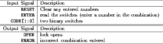
You are building the controller for a 2-bit serial lock used to control entry to a locked room. The lock has a RESET button, an ENTER button, and two two-position switches, CODE1 and CODE0, for entering the combination. For example, if the combination is 01-11, someone opening the lock would first set the two switches to 01 (CODE1 = low, CODE0 = high) and press ENTER. Then she would set the two switches to 11 (CODE1 = high, CODE0 = high) and press ENTER. This would cause the circuitry to assert the OPEN signal, causing an electromechanical relay to be released and allowing the door to open. Our lock is insecure with only sixteen different combinations; think about how it might be extended.
If the person trying to open the lock makes a mistake entering the switch combination, s/he can restart the process by pressing RESET. If s/he enters a wrong sequence, the circuitry would assert the ERROR signal, illuminating an error light. S/he must press RESET to start the process over.
In this lab, you will enter a design for the lock's controller, in a new Workview project. Create a lab2 folder in your home directory. Then make a new Workview project in the lab2 folder. Make RESET and ENTER inputs. Simulate pressing the ENTER button by forcing it high for a clock cycle. Use a two-bit wide input bus called CODE[1:0] for the two switches. (Refer to a later section for information on busses in Workview.) The outputs are an OPEN signal and an ERROR signal.
Figure 1 shows a decomposition of the combination lock controller, whose inputs and outputs are
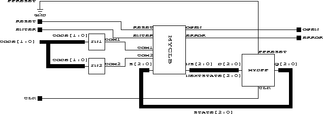
Figure 1: Controller for the Combination Lock
Blocks IN1 and IN2 process the input signals COM1 (COMpare 1) and COM2 (COMpare 2) into a simpler form for the FSM. Specifically, COM1 is asserted when CODE[1:0] is the combination's first number. Similarly, COM2 is asserted for the second number. Partitioning the circuit this way makes the combination easy to change.
Choose your own combination; the two numbers must be different.
This should be a simple block. Use a few AND gates and inverters.
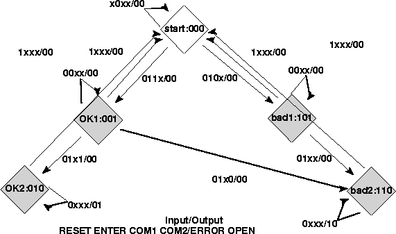
Figure 2: State Transition Diagram
The MYCLB (MY Combinational Logic Block) block takes RESET, ENTER, COM1, COM2, and present state and generates OPEN and ERROR, as well as the next state. Figure 2 shows the state transition diagram, a Mealy machine since the transitions are labeled with both inputs and outputs. The white circle denotes the reset state (i.e., the state the machine starts in).
By writing an ``AND'' term describing each row where an output is 1 and ORing these together, it's easy to obtain a set of equations implementing this, as shown in Figure 3.
Translating a state transition diagram to a truth table is mechanical: write a row for each transition. In Figure 4a, I've collapsed a few rows together by noting that when reset is 1, the outputs and next state are the same for all states. Note RESET' means NOT RESET.
Implementing the equations of Figure 4a as written would be inefficient, so we introduce intermediate variables T0,...,T6 as shown in Figure 4b. Make symbol and schematic for MYCLB using the equations in Figure 4b.
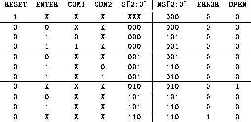
Figure 3: Truth Table for the FSM
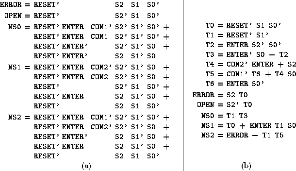
Figure 4: Logic Equations for the FSM (Unoptimized): (a) two-level (b) multi-level
Create a block called MYDFF that contains three D flip-flops (one for each state bit) with an asynchronous clear hooked to a pin called FFRESET (Flip-Flops RESET). The flip flops you should use are the FDC (D Flip-flop with asynchronous Clear) flip flops. Externally, connect FFRESET to 0 (i.e., not resetting), but during simulation, you can force this to 1 to reset every flip-flop.
ViewDraw supports busses, collections of wires drawn as one, through the bus button. An eight-bit data bus, for example, might be labeled DATA[7:0]. A net connected to a bus ``breaks out'' one of the bus signal--labels. To connect a net to a bus, you need to name the net with the name of the broken-out signal, e.g., DATA5. It's also possible to break out sub-busses, e.g., DATA[5:2].
All busses must be labeled so ViewDraw knows their width (how many wires), even those passing directly from one component to another where there is (seemingly) no ambiguity about the width.
Pins on symbols can accept busses: label the pins with a bus name (i.e., using the bracket notation).
Bussing related signals makes the circuit easier to read and simulate. In ViewSim, vector data DATA[7:0] (or v data...) makes the signals DATA7, DATA6,...,DATA0 into a vector called data, which can be treated like any other signal: you can watch vectors, you can use them with the wave command. Use the assign command to set a vector's value. E.g., a data 3e&#;'134 h (hexadecimal) or a data 00111110&#;'134 b (binary).
Use a bus for the inputs and outputs of the state register (MYDFF) and the state inputs and outputs of the combinational logic block (MYCLB).
In addition to inputs, ViewSim allows you to force internal signals, those normally driven by components, to particular values. For example, you've tied FFRESET to 0, but it can be set high simply by typing h FFRESET, which will reset the state bits to zero after you simulate for a step. Use r FFRESET to release the signal--return it to its default.
A similar trick lets you set the state to anything you want. Simply set NEXTSTATE[2:0] to the state you want, clock the FSM, and then release NEXTSTATE[2:0].
ViewSim allows you to define clocks, input signals that change periodically. For example, clock clk 0 1 makes the signal clk oscillate as the circuit is simulated. To simulate for a single clock period, use cycle instead of sim. Watched variables in ViewSim are not displayed with cycle, but those displayed with the wave command in ViewTrace are updated.
In ViewSim, when the name of a command file is invoked, the contents of the file are interpreted as if you typed them one by one. You may create the file by using edit, a MS-DOS editor, or by using WordPad, a Window-NT text editor.
To use edit, first get a Command Prompt from the Start menu under Programs. Then change to your project directory with the cd command. Then edit your command file with edit yourfile.cmd.
To use WordPad, make sure that you save your yourfile.cmd as text.You can get a WordPad from the Start menu under Programs, under Accessories.
In ViewSim, you can create a transcript of your work using the command log. Start a log with log filename.log, and end a log by typing log alone.
Workview, DOS, and Windows is case-insensitive, somewhat, although we've used all caps for signals throughout this handout.
You may use letters, numbers, and underscores (_) in filenames. The period (.) may only appear in certain places (e.g., yourfile.cmd, MYCLB.1, etc). Avoid other punctuation. Since you will use some DOS programs later, make your file names be no more than 8 characters. Follow this convention for naming all your components as well.
You may use letters, numbers, and underscores in labels, but avoid other punctuation except for bus notation: [:].
Do not use names already used by components in other libraries. For example, do not call your combinational logic block CLB since there is already a component with that name in the (xc4000e) library.
Name:Name:
Lab Section (Check one)
M: 11 12 T: 13 W: 14 15 Th: 16
Design the IN1, IN2, and MYCLB blocks. Enter it in ViewDraw using only components from the (xc4000e) library. You'll probably use the AND2, AND3, OR2, OR3, INV, FDC, and GND components.
TA: (20%)
Make a test script for your CLB and run it. Show the TA your script and that the output is correct.
TA: (20%)
Design your state register using D-Flip Flops. Call it MYDFF.
TA: (10%)
Wire up the FSM using the CLB and state register you designed.
TA: (20%)
Write a ViewSim command file to simulate the following scenarios:
Create a log file to show your TA.
TA: (30%)
Turned in on time
TA: (full credit 100%)
Turned In One Week Late
TA: (1/2 credit of your Points%)
Bonus: Where is the critical path (longest propagation delay)? Calculate the longest propagation delay on paper assuming unit delay for each gate.
TA: (2%)
Lab 2
This document was generated using the LaTeX2HTML translator Version 96.1 (Feb 5, 1996) Copyright © 1993, 1994, 1995, 1996, Nikos Drakos, Computer Based Learning Unit, University of Leeds.
The command line arguments were:
latex2html -split 0 lab2.tex.
The translation was initiated by CS 150 Instructor on Tue Jan 27 19:11:58 PST 1998