CS61C Homework 4
Synchronyous Digital Systems
| Due: | 2008.07.25 @ 11:59pm |
|---|---|
| TA: | Omar Akkawi <cs61c-tl@imail.eecs.berkeley.edu> |
Background
Goals
This assignment will check your understanding of synchronous digital systems, state elements, and combinational logic.
Assignment
Question 1
What is Moore's law? The Intel Pentium 4 Prescott (3.6 Ghz version), released in 2004, has roughly 125,000,000 transistors on the chip. This chip can perform about 7,000 MIPS (Millions of Instruction Per Second). Based on this information and your knowledge of Moore's law, how many transistors do you think the Intel 8088, which was released in 1979, had on the chip? What would you estimate the MIPS rating of this chip to be?
Question 2
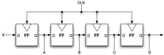
Consider the circuit of Flip-Flops (FF) shown here. Assume that input X alternates between 1 and 0, changing at the falling edge of each 50 ns clock period and initializing as 0. Draw the detailed wave for the clock signal, input X, and the signals at points A, B, C, and D in the circuit for the first 6 clock cycles. Assume that the clk-to-q delay is 7ns. Show undetermined signals as shaded bars for the duration that is undetermined. You may optionally show clk-to-q as dotted lines if it helps you.

Question 3
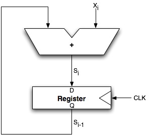
Consider the accumulator discussed in the readings and presented in class. Given the following: The adder propagation delay is 2ns, the register setup time is 1 ns, the register clk-to-q is 1ns, and the clock frequency is 500MHz. Will the accumulator function correctly? If not, what would you suggest changing to fix the problem?
Question 4
Design a finite state machine (FSM) with the following behavior: Inputs arrive one bit at a time, one bit per clock cycle. The FSM outputs a 1 if the pattern '011' has been recognized and continues to output a 1 as long as bits matching that pattern continue to be input. The FSM should output 0 at all other times. ie. '011011011...' will continue to output 1 after it starts to do so, but '011001...' will output '001100', which stops outputting 1 when the pattern first deviates. Your FSM should include a start state and a diagram entry arrow, but no end state is needed (or warranted).
This is a three steps design.
- draw the state diagram
- specify the truth table for (current state and input) -> (next state and output)
- devise the logic gate circuit-level implementation for the lowest bit of next state as a circuit with input current state bits and input (note that you can make the circuit implementation of each next state bit and output using the same techniques)
Question 5
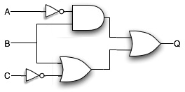
Derive the truth-table for the CL circuit shown here. (Remember, you do this by applying all possible input combinations, one at a time). What is the most simplified version of the expression that this circuit/truth-table generates?
Question 6
Write the canonical sum-of-products form of a Boolean expressions for a 4 input function whose output is 1 if and only if the number of 1's in the input is even.
Question 7
Write the most simplified Boolean expression for the function
represented by the truth-table below. SHOW ALL YOUR WORK! The solution
is the OR of three AND terms, each with 2 variables.
(Note: If you are up for a little extra reading, check out K-maps)
| ABC | Y |
|---|---|
| 000 | 1 |
| 001 | 0 |
| 010 | 1 |
| 011 | 0 |
| 100 | 0 |
| 101 | 1 |
| 110 | 1 |
| 111 | 1 |
Question 8 - Optional
Redraw the complete UNSIMPLIFIED circuit diagram from problem 5 using only NAND gates. You must show all the gates used (that is to say, you can not include larger structures in your diagram). Show all your work to derive this structure.
Submission Details
Create a directory named 'hw4' containing a README and any additional files needed for your submission. The README should say where to look for each question's solution. While in that directory, run 'submit hw4'. If you included an image, make sure to say "yes" when the submit script prompts you about it. Please only submit images in the following formats: GIF, JPG, and PDF.