Due Wednesday, August 6, 2008 at 11:59pm
TAs: Albert ChaeClarifications to spec will be posted in red.
Post any questions or comments to the newsgroup.
Overview
In this project you will be using Logisim to create a 16-bit single cycle CPU. This project does not involve pipelining or caches, so make sure you don't confuse ideas of CPU design that are drawn from those topics. Please read this document CAREFULLY as there are key differences between the CPU we studied in class and the CPU you will be designing for this project.
Instruction Set Architecture (ISA)
You will be implementing a simple 16-bit processor with four registers ($r0 through $r3). It will have separate data and instruction memory. Because this is a 16-bit architecture, our words are 16 bits wide, unlike the 32-bit MIPS we have been studying in class. For the remainder of this document, a WORD refers to 16 bits. Each of the four registers is big enough to hold ONE word.
IMPORTANT: Because of the limitations of Logisim and to make things simpler, our memory will be WORD (16 bit) addressed, unlike MIPS which allows you to address each byte individually.
The instruction encoding is given below. Your processor will pull out a 16-bit value from instruction memory and determine the meaning of that instruction by looking at the opcode (the top four bits, which are bits 15-12). If the instruction is an R-type (i.e. opcode == 0), then you must also look at the funct field.
Note how we did not fill up the following table with 16 instructions as is possible with 4 bits of opcode, nor did we have 64 R-Type instructions with 6 bits of funct. This way the project is shorter and easier.
| 15-12 | 11 | 10 | 9 | 8 | 7 | 6 | 5 | 4 | 3 | 2 | 1 | 0 | |
|---|---|---|---|---|---|---|---|---|---|---|---|---|---|
| 0 | rs | rt | rd | funct | See R-type Instructions | ||||||||
| 1 | rs | rt | immediate (unsigned) | disp: DISP[imm] = $rs | |||||||||
| 2 | rs | rt | immediate (unsigned) | lui: $rt = imm << 8 | |||||||||
| 3 | rs | rt | immediate (unsigned) | ori: $rt = $rs | imm | |||||||||
| 4 | rs | rt | immediate (signed) | lw: $rt = MEM[$rs + imm] | |||||||||
| 5 | rs | rt | immediate (signed) | sw: MEM[$rs+imm] = $rt | |||||||||
| 6 | target address | jump | |||||||||||
| 7 | rs | rt | offset (signed) | beq | |||||||||
| 8 | rs | rt | offset (signed) | bne | |||||||||
R-Type Instructions
| funct | meaning |
|---|---|
| 0 | or: $rd = $rs | $rt |
| 1 | and: $rd = $rs & $rt |
| 2 | add: $rd = $rs + $rt |
| 3 | sub: $rd = $rs - $rt |
| 4 | sllv: $rd = $rs << $rt |
| 5 | srlv: $rd = $rs >> $rt |
| 6 | xor: $rd = $rs ^ $rt |
| 7 | slt: $rd = ($rs < $rt) ? 1 : 0 |
NOTE: These instructions and their select values
are the same as your ALU from hw5 except for
6 = 0b110
which we will now use for the xor instruction. I replaced
sra partly because it is somewhat of a hassle to do it using library
circuits, but more because xor gives us the ability to
zero out registers as well as do bitwise negation. Also, we
do not care about either overflow for this project.
jump
The jump instruction's argument is a pseudoabsolute address, just as in MIPS. address is an unsigned number representing the lower 12 bits of the next instruction to be executed. The upper four bits are taken from the current PC. We do NOT do any concatenation of zeroes to the bottom or our address like we would in MIPS. This is because our CPU is be WORD addressed, so every possible address holds a valid 16 bit instruction.
PC = (PC & 0xF000) | target address
beq/bne
The beq instruction's argument is a signed offset relative to the next instruction to be executed if we don't take the branch, which is similar to MIPS. Note that the address of this next instruction is (PC+1) rather than (PC+4) because our CPU is WORD addressed. beq can be represented as the following:
        if $r0 == $r1
                PC = PC + 1 + offset
        else
                PC = PC + 1
The bne instruction differs only by the test in the if statement: replace the == with !=
immediate Fields
Note that the immediate field is only 8 bits wide, so we must perform some kind of extension on it before passing it to the ALU. If an immediate is supposeed to be unsigned, be sure to zero-extend it. If an immediate is signed, be sure to sign-extend it.
Logisim
It is strongly recommended that you download and run Logisim on your local machine while developing your CPU. As you've probably discovered in lab, Logisim can quickly overwhelm the instructional machines. Though Logisim is relatively stable compared to Spring 2005, it is still recommended that you save often and also make backup copies of your .circ files early and often. The official version of Logisim we will be using for evaluation is v2.1.6.
If you are having trouble with Logisim: RESTART IT and RELOAD your circuit! Don't waste your time chasing a bug that is not your fault. However, if rebooting doesn't solve the problem, it is more likely that the bug is a flaw in your code. Please post to the newsgroup about any crazy bugs that you find and we will investigate.
RAM Modules
Logisim RAM modules can be found in the built-in memory library. To add the library to your project, select "Project/Load Library/Built-in Library..." and select the Memory module.
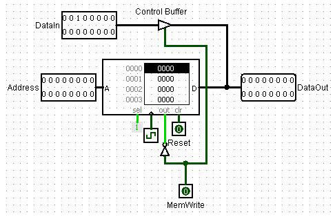
Because the RAM module doesn't look like the idealized memory we saw in lecture, you may feel confused about where to begin. The picture above shows a good way to wire up a circuit to use RAM. Here are a few things to know before you get started.
- "sel" determines whether or not the RAM module is active (if "sel" is low, "D" is undefined). We will probably not run into any cases where we need to turn our RAM off, so you can wire a constant 1 to this.
- "A" chooses which address will be accessed.
- The clock input provides synchronization for memory writes. Be sure to use the same clock here as you do for your reg file.
- "out" determines whether we are reading or writing to memory. If "out" is high, then "D" will be driven with the contents of memory at address "A".
- "clr" will instantly set all contents of memory to 0 if high. You should wire a manual switch so you can clear out memory whenever you want to restart a test.
- "D" acts as both data in and data out for this module. This means you have to be careful not to drive this line from two conflicting sources, which in this case are DataIn and the output of the memory. You can solve this by using a controlled buffer (aka a tri-state buffer) on the "D" port of the RAM module. By wiring logic to the "out" port and the valve port of the controlled buffer together so that they are always opposite values (as in the picture above), we can prevent conflicts between data being driven in and the contents of memory coming out.
- The "poke" tool can be used to modify the contents of the memory. You can also use right-click --> Load Image... to load an image from a file.
Use a RAM module for Data memory and a Logisim ROM module for your instruction memory. It is a much simplified version of a RAM module and thus it should be easy to pick up after figuring out RAM.
The Display Instruction
Remember that the five components of a computer are control, datapath, memory, input, and output devices. Unfortunately, we won't have much input besides loading to memory. But we will have a cool output device using 7-segment LEDS.
We provide for you a converter circuit (right click and save as) that converts 16 bits into 4 hex digits, which are displayed on a "bundle" of four 7-segment LEDs. Each bundle should look like the following:
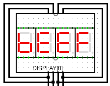
Your project must include an array of at least two of these display "bundles" for output. You may wish to add more so you can have more interesting output, but we will only require two. Remember that the disp instruction takes the value in $rs and displays it on the immth "bundle". This means you will only care about as many immediate values as you have display bundles to show them on.
Your bundles may display 0000 or any other garbage before any
disp instructions have been executed.
They must hold their values until another disp instruction replaces
the value in that bundle.
For example:
    xor $r0, $r0, $r0
    disp $r0, 0   # At this moment, DISP[0] should show 0000

    ori $r0, $r0, 0x1   # DISP[0] should still show 0000
    add $r0, $r0, $r0   # DISP[0] should stlll show 0000

    disp $r0, 0   # DISP[0] should now show 0002
This means you will need to add some form of state for each
display bundle. It is acceptable if the value on the display
does not actually change until the rising edge of the next
clock cycle.
Testing
Once you've implemented your CPU, you can test it's correctness by writing programs to run on it! First, try this simple program as a sanity check: halt.hex. This program loads the same immediate into two different registers using lui/ori and then branches -1 if these registers are equal.
         lui $r0, 0x33          2033
         ori $r0, $r0, 0x44     3044
         lui $r1, 0x33          2133
         ori $r1, $r1, 0x44     3544
         beq $r0, $r1, -1       71FF
For practice, verify that the assembly on the left matches
the translated binary on the right. This program effectively "halts"
the CPU by putting it into an infinite loop, so you can
observe the outputs as well as memory and register state. Of
course, you could do this "halt" with only the beq line, but
it is very important that you test your lui/ori
or the programs we will use during grading will not work.
You are required to write 2 sample programs to test your CPU, but you should also write others to test all your instructions
- Write a program that multiplies the first two words of memory (MEM[0] and MEM[1]) and stores their product in MEM[2]. You may treat MEM[0] and MEM[1] as unsigned values. Also, do not worry about the case where the product does not fit in 16 bits. The last instruction of your program must be a halt (an instruction that jumps or branches to itself indefinitely). Feel free to clobber the original arguments. Save the ROM image in a file "mult.hex."
- Write a program that displays the lower nine bits of the first word of memory in octal (base 8). For example, if the first word were 0x829f, the seven segment displays would read 0237. Again, you may clobber any memory values you like and your program must end with a halt. Save the ROM image in a file "octal.hex".
Assembler
It's a good idea to assemble some of your programs by hand
for the practice. This gets tedious, however, so I will provide
more info about an assembler here later
I've uploaded a basic assembler to ~cs61c-tj/public_html/proj3asm. You can run it with
~cs61c-tj/public_html/proj3asm/assembler.py < input_file > output_file
A sample input file is provided: ~cs61c-tj/public_html/proj3asm/sample.s
This file shows examples of proper syntax and what kind of comments are supported.
If you find any bugs, please notify Albert right away! Also, your fellow students have been writing/posting their own assemblers to the newsgroup. It sounds like most of these have better/more features, so you should definitely check them out.
"Features"
- No error checking.
- Jumps/branches can't take labels.
- Jump address can be unsigned hex or decimal.
- Branch offset is signed decimal only.
- lw/sw offset is signed decimal only.
- lui/ori only support 8 bit immediates, but they can be unsigned hex or decimal.
- disp immediate only takes unsigned decimal.
Miscellaneous remarks
This section contains some comments to help you get started and foster some academic debate. Feel free to skip this section for now and come back after you've gotten your hands dirty.Questions to Think About
1) What instructions (and with what arguments) can act as nops?2) What are the different ways of halting a program?
3) How can we implement Multiplication? Division? (in software, not hardware)
Logisim's Combination Analysis Feature
Logisim offers some functionality for automating circuit implementation given a truth table, or vice versa. Though not disallowed (enforcing such a requirement is impractical), use of this feature is discouraged. Remember that you will not be allowed to have a laptop running Logisim on the final.
Key Differences From MIPS
1) The zero register isn't special. $r0 is just a regular register like $r1.2) Memory is addressed every 16 bits, or a WORD in our 16 bit architecture. That means each location in memory holds a 16 bit value, unlike MIPS where each location holds 8 bits.
3) Data memory and instruction memory are separate. Remember that in MIPS, we create the illusion of separate memory with two caches, but we really have only one memory.
Miscellaneous Requirements
Do not gate the clock! This is very bad design practice when making real circuits, so we will discourage you from doing this by heavily penalizing your project if you gate your clock.
You may use any built-in logisim library circuit components in implementing your CPU.
You must have your instruction ROM module and data RAM module visible from the main circuit of your Logisim project. You must include an array of at least two seven segment display bundles in the main circuit as well. Anything else can go in subcircuits. Feel free to add additional seven segment displays if it does not clutter your CPU.
Use the label tool to organize your CPU. In particular label the control, datapath, and display sections, but it can also be useful to label specific busses and wires. It could make debugging a lot easier!
Plan
If you are feeling overwhelmed by this spec, these steps may help you get started. These are only suggestions, and you can choose to make any adjustments you prefer. For example, some of you may want to design the control before the datapath. Just remember to follow the rule above about keeping both memories and the display bundles at the top level main circuit.
- Unfortunately because of Logisim's problem with complex nested circuits, you should rebuild an ALU using library circuits rather than reuse your HW5. This should be a lot easier than the homework because you don't have to build everything from scratch. Remember that this ALU has a bitwise XOR instead of SRA and that we aren't going to worry about overflow.
- You should familiarize yourself with how Logisim's RAM and ROM modules work. Follow the guidelines in the section "RAM Modules" above.
- If you haven't already, you should familiarize yourself with how Logisim's Registers work. Once you are comfortable with this, you should try to build a register file. Remember to analyze the ISA to see what it requires from this register file. You may want to build this register file at the top level circuit or maybe as a subcircuit.
- Think about any other components you will need in your datapath. Build these, and then layout everything. Wire these components together so that this datapath can execute every instruction our ISA supports. Be sure to identify any control signals you will need to generate.
- Design your control. Remember the process we discussed in class.
- Connect the control to the datapath.
- Test instructions individually, then try whole programs.
- Finish writing "mult.hex" and "octal.hex".
- Submit your cpu and programs
- Rejoice! and then start proj4.
Extra for Experts
Once you've got your CPU up and running, give these a try: (BACKUP your completed CPU first)
- Add more features to the assembler.
- Try writing a program that divides MEM[0] by MEM[1] and stores the quotient in MEM[2] and the remainder in MEM[3].
- Use your program from part 2 to write a program that displays a location in memory as a decimal value! (be careful about jumps, playing linker can be tough).
- Add several display bundles and write life1D!
- Write something crazy that we haven't thought of.
Submission
You must submit the following files:cpu.circ
mult.hex
octal.hex
From the directory containing your project files, submit using the following command:
% submit proj3