The system of Boolean algebra (invented by the mathematician George Boole in the 19th century) allows us to manipulate Boolean expressions to make the circuits that implement them faster, smaller, or cheaper. (Remember, in logic &bull is AND and + is OR. In C, the bitwise versions of these are & and |.)
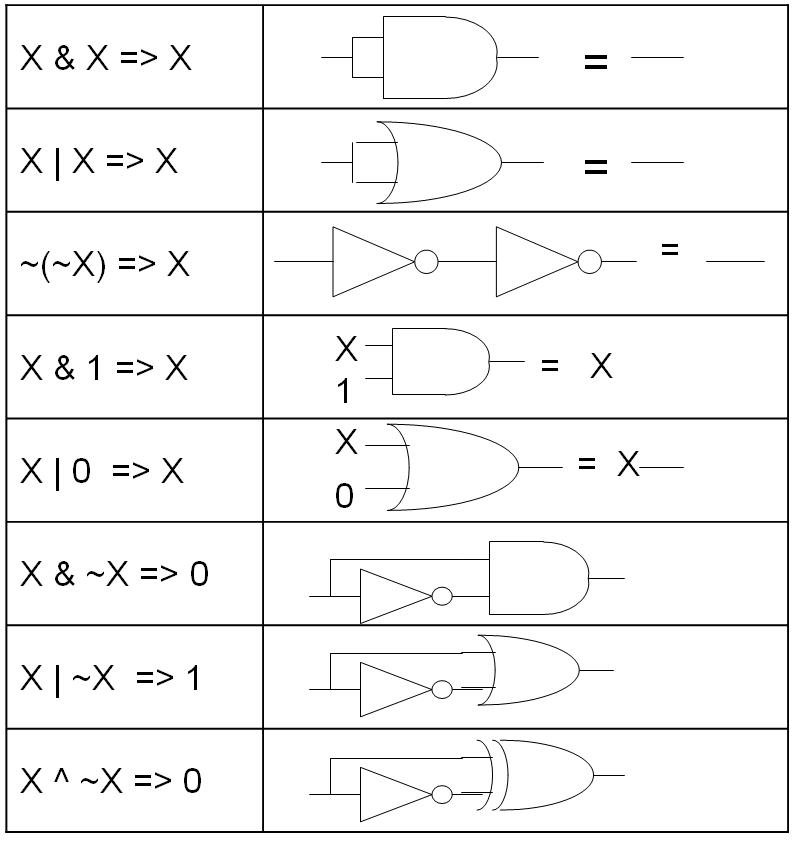
Listed below are useful laws of Boolean algebra.
x • !x = 0 x • 0 = 0 x • 1 = x x • x = x x • y = y • x (x • y) • z = x • (y • z) x • (y + z) = x•y + x•z x•y + x = x !(x•y) = !x + !y |
x + !x = 1 x + 1 = 1 x + 0 = x x + x = x x + y = y + x (x + y) + z = x + (y + z) x + y•z = (x + y) • (x + z) (x + y) • x = x !(x + y) = !x • !y |
complementarity laws of 0's and 1's identities idempotent law commutativity associativity distribution uniting theorem DeMorgan's law |
Notice that all these laws come in two versions, one being called the dual of the other. Practically speakinng, this means you if you know one version of the law and the other one can be easily derived.
Here is an example of using these laws to simplify the expression y = a•b + a + c.
| y = a•b + a + c | |
| = a•(b+1) + c | distribution, identity |
| = a•1 + c | law of 1's |
| = a + c | identity |
An alternative expression for a xor b is (a + b)•(!a + !b). Show that this expression is equivalent to the one previously presented, a xor b = a•!b + !a•b.
Using the laws of Boolean algebra, show that a + !a•x = a + x. (This means we can eliminate two of the three gates without changing the behavior of the circuit!)
Supply the steps that simplify
y = !a • !b • !c + !a • !b • c + !a • b • c + a • !b • !c +a • b • !c
to
!a•!b + !a•c + a•!c
These transformations can be done algebraicly or graphically. Many of them seem obvious, but when you have 100s of millions of gates, having tools that perform these zillions of little optimizations for you, without making any mistakes, is a huge benefit. Here's some simple examples that eliminate unnecessary gates.
((X & Y) & A) & B => (X & Y) & (A & B)
(X & A) | (A & B) => (X | Y) & A)
(x & A) | (~x & A) => AThis allows you to take the AND gates in the SOP coming from two ON rows in a truth table that differ by complementing one input and smash them together. It eliminates two AND gates and one input to the OR gate. In EECS150 you learn a clever trick for this called Karnaugh maps. In CAD courses you learn even more powerful algorithms for this.
Given below is the truth table for the majority function. It takes three inputs, and returns whatever value two or more of the inputs share.
a b c  m
0 0 0  0
0 0 1  0
0 1 0  0
0 1 1  1
1 0 0  0
1 0 1  1
1 1 0  1
1 1 1  1
Devise an implementation with as few gates as possible (our version has three AND's and two OR's), and implement your solution in Logisim.
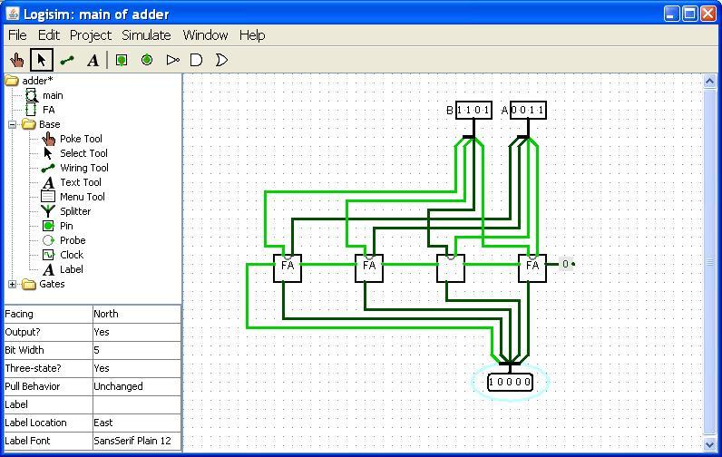
Copy ~cs61cl/code/adder.circ to a local directory and open it up with logisim. Double click FA to focus on the FA subcircuit. Do Project->Analyze Circuit. (You will see that the inputs and truth table and expressions all reflect the input and output labels.) This time when you Build Circuit make the name FA2 and click the "Use Two-Input Gates Only" box. Take a look at the new circuit that you have, called FA2.
The behavior of FA and FA2 is identical. Poke it and try it out. Workng with subcircuits
In fact, you could replace FAs with FA2s in main. But one thing you need to be careful about is the layout of pins on the subcircuit symbol. Try dropping an FA2 in main somewhere. See, it has three pins on the left (the inputs) and two on the right (the outputs). You need to be extremely careful if you change the pins in a subcircuit in any way. (In case we didn't say it strong enough. BEWARE. Modularity through subcircuits is incredibly powerful. But, you must establish the interface to the module and keep it.)
Rearrange the pins on your FA2 module so that they conform to the orientation in FA. Note, when you mouse over the pins on the symbol you can see their names. When you've got it right, rip out an FA and replace it with an FA2. Poke at it to verify that it is still a 4-bit adder.
A B nand(A,B)
0 0 1
0 1 1
1 0 1
1 1 0
In the last lab, you saw that this funny gate is actually more powerful than the three more familiar ones - it is complete all by itself. Any logic function can be constructed using only NANDs. Perhaps even more surprising is that it is a lot faster and smaller than an AND gate or and OR gate. It seems that transitors just really like this idea of complementing the output. NOR is complete, fast, and small as well.
Well, if that hasn't got you excited about NAND, there's more. You may have run into De Morgan's law. It has two forms.
A + B = ~(~A • ~B)
A &bull B = ~(~A + ~B)
To prove the first one, construct the truth table for the to side and check if they are the same.
A  B  A+B   ~A  ~B  (~A & ~B)  ~(~A & ~B)
0  0   0     1   1      1          0
0  1   1     1   0      0          1
1  0   1     0   1      0          1
1  1   1     0   0      0          1
Look at what this does with a Sum of Product circuit. The OR is replaced with a NAND and a bubble (complement) is place on each of its inputs. Slide the bubble back to the AND gate. Sum of products is a NAND of NANDS!
Go back to your FA subcircuit and run Project->Analyze Circuit. This time when you run build circuit click the "use only nand gates" and give it a new name.
Start a new project, drop in three input pins and one out put. Click on the pin to bring up the properties in the the lower left portion. Update the labels to reflect the names used in the columns of the truth table for the majority function. Enter in the truth table. Take a look at the expression. Did it find the same optimizations that you did? Build the circuit. Build it again using 2-input gates.
A decoder does the reverse. It converts a binary input into a unary output. However, instead of the number of fingers it is the position of the finger that gives the value. (Yes, counting on your fingers is a very inefficient number system!) The truth value for a 2-bit decoder is giveb below. Create a new project can implement this decoder using logic gates.
S1 S0 | D3 D2 D1 D0
0  0  | 0  0  0  1
0  1  | 0  0  1  0
1  0  | 0  1  0  0
1  1  | 1  0  0  0
It should have four data outputs, d0, d1, d2, d3 on the right side, and two control inputs, s1 and s0. When you are done, you can compare your solution to the one in ~cs61cl/code/decoder.circ. One new bit of logisim that you will want. Click on gates in the explorer panel on the left. In there you will see a constant.
In the homework for the last lab you constructed a 2-1 Multiplexor (MUX) and then built a 4-1 multiplexor using 2-1 MUXes. The other name for a multiplexor is a selector. The control inputs select one of the data inputs to appear on the output. We will used these a lot. If you haven't done that exercise already, you will probably want to do it now.
A demultiplexor is the inverse of a multiplexor. It steers the input to the one of 2^n outputs that is specified by the n control inputs. Modify your decoder to that it becomes a demultiplexor. The truth table for this demultiplexor is the following. But in this case, you will find it easier to think structurally and just steer the input to the correct output, rather than cranking through the truth table.
S1 S0 IN | D3 D2 D1 D0
0  0   0 | 0  0  0  0
0  0   1 | 0  0  0  1
0  1   0 | 0  0  0  0
0  1   1 | 0  0  1  0
1  0   0 | 0  0  0  0
1  0   1 | 0  1  0  0
1  1   0 | 0  0  0  0
1  1   1 | 1  0  0  0
Logisim handles this duality with two mechanisms. First, the splitter tool can either take several individual signals and group them together into a bundle or split a bundle into its individual signals. Second, each input to a gate can have a bit width, as well as a number of inputs. So far, all our inputs were one bit wide. The logical symbols can be used on every signal in a bundle. This is a little like the bit-wise operators in C (&, |, and ^), as they do a bit-wise logical operation on each bit in the (scalar) object, i.e., char or int.
Let's first use the concept of a data bus on your four bit adder. Open it up under logisim and remove the individual input pins and output pins. (Grab the select tool, right click on the object and select delete or select a region and cut.) Under the Base menu, grab the splitter tool. Change its properties so that it faces south and has a bit width of 4 and a fanout of four. Drop this above you 4-bit adder built out of FAs. Attach a wire to the top, i.e, the 4-bit wide part. Grab the input pin tool, set it to be south facing and four bits wide. Attach it to your wire and label it A. Attach the individual signals to the A input of your FAs.
Do the same for the B side.
Grab the splitter again, but make it North facing with a bit width of 5 and an fanout of 5. (This is a bit of a misnomer, because it will really be a fan-in).
Why does it need to be five bits wide? What is the fifth bit?
Connect the sum output and the carry out to you unsplitter and put a 5-wide output pin on it facing north. It should look something like what is below. Poke the inputs. Now this adds binary numbers, rather than a bunch of bits.
While you've got the Base menu open, notice the Probe tool. This is your debugging friend. Grab it and drop it on each of the internal carrys. Poke the inputs to see that it is showing you whats going on. Here you get the same information as the highlighting on the signal. But you can make the probe multiple bits wide and drop it on busses. Try it.
Now we can move up one level of design. The Logism gates are really a library of gates of different sizes and widths. You know how to build multiplexors and complex boolean functions out of individual logic gates. Logisim provides a library of the larger devices too. Go to Project->Load Library->Built-in Library and select Plexers. Open that up. See some familiar parts.
Let's build a simple 16-bit logic unit. It has four functions: AND, OR, XOR, EQ. It has two 16-bit inputs: A and B, and one 16-bit output, R. It has a 2-bit control input OP that selects which function is performed, according to the following table.
OP  Function
00  AND
01  OR
10  XOR
11  EQ
Build this using four 16-bit wide logic gates and one 16-bit wide multiplexor.
A:   1 1 0 1    (13)
B:  -0 0 1 1     (3)
    --------
c:   1 0 1 0    (10)
Using seven FAs, construct a circuit that takes 8 input bits and produces a 4-bit binary output that is the number of 1s in the input. This is a different kind of unary-to-binary conversion.