The synchronous design methodology was introduced last week in lecture and is explained in much greater detail in this lab. In this approach, digital systems are constructed using two kinds of circuit elements: combinational gates and storage elements. All feedbacks from outputs to inputs must go through a storage element. There is a special signal, called the clock that allows the storage elements to capture and hold onto their inputs. Whenever the clock ticks, all the storage elements grab their inputs and record them internally. Soon afterwards, the new inputs will be visible on the outputs of the storage elements, whereupon they feed into the inputs of combinational logic and propagate along until they reach the input of a storage element. There, the value sits unheeded until the clock ticks again.
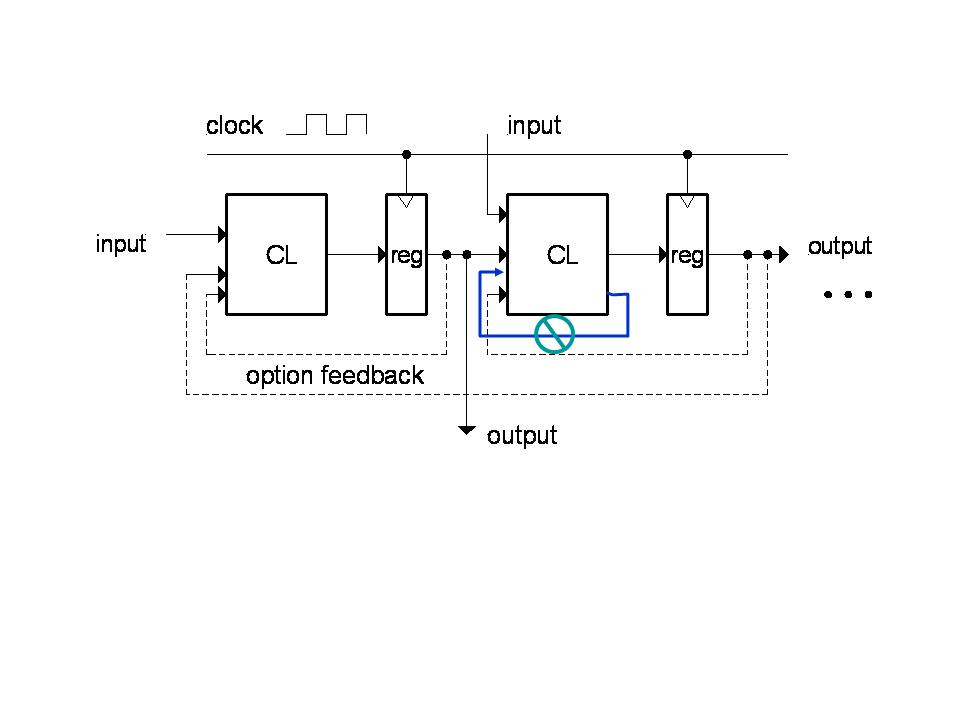
A schema for this style of design is shown in the figure below. Acyclic blocks of combinational logic take their inputs from synchronous storage elements, called registers, and their outputs feed into registers. All cycles in the circuit include at least one register. When the clock ticks the entire state of the system is updated.
Often the performance of a digital system is indicated by its clock frequency, called the clock rate. For example, current PCs run at a little more than 3 GHz, that is 3 billion clock cycles per second. The clock cycle time must be long enough to accomdate the longest propagation delay from any register output to any input. A typical rule of thumb is that the circuit should be designed so that this is roughly 10 levels of logic. So, at 3.3 GHz, the clock cycle is 300 picoseconds, that allows for 30 picosends of propagation per gate. Actually, speed of light takes almost 100 picoseconds to cross the width of a large ship, so the allowed gate delay is more like 15 picoseconds. Pretty fast.
The the table that you are looking at is a waveform - a sequence of values over time. Here time is going down vertically and it only shows the changes. When you change the input it simulates the circuit till the output is determined. Here, that is always 0.
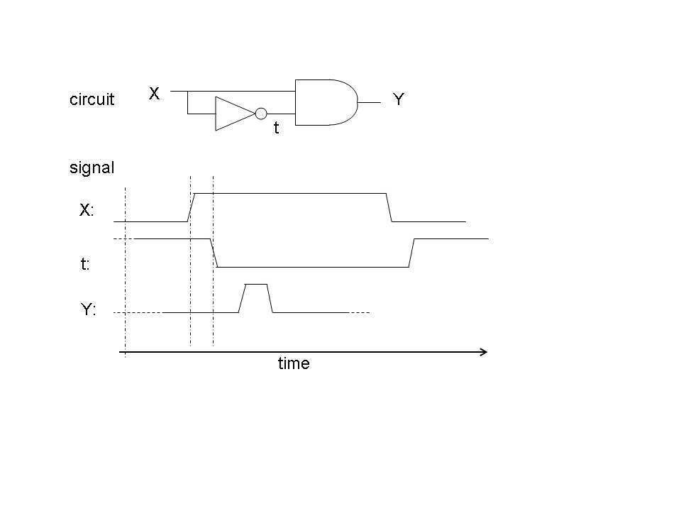
If you had a real AND gate and INV gate and hooked them up to an oscilloscope to watch the voltage on various signals over time, the waveform for X would look like the top graph in the figure above. It is zero for a while and at some time you raised it to 1 and then later you lowered it to 0. However, if you were to to look at Y, you would see that just a tiny tiny time after you raised X there is a little glitch where Y goes to 1. This is because gates take time. If you were to look inside at the intermediate signal t, it would look like an inverted version of X, except that it is delayed by one gate delay. This means that for on gate delay (perhaps 15 picoseconds) both X and t are equal to 1! A gate delay later this will appear at the output Y, but it will dissappear one gate delay later.
Question: what will happen when X is dropped to zero again?
out == ~~~out == ~out.
The output cannot settle; if it settled to 1 it would need to be 0 and if it settled to 0 it would need to be 1. Watch what happens when you poke the input to 1.
Logisim detects the cycle, marks it as inconsistent, and refuses to simulate it. If you wired it up in the lab, it will do something. It won't blow up. Based on what you saw in the glitch, what do you think this circuit will do?
The basic cicuit element that holds state is a flip-flop. The name comes from its behavior - it can flip from one state to another and hold it. In order to use flip-flops, we introduce a special waveform, called a clock, that oscillates (or ticks) with a well-defined period. In fact, we engineer the clock so that it looks like a periodic square wave and its edges are carefully engineered to be the same throughout the design.
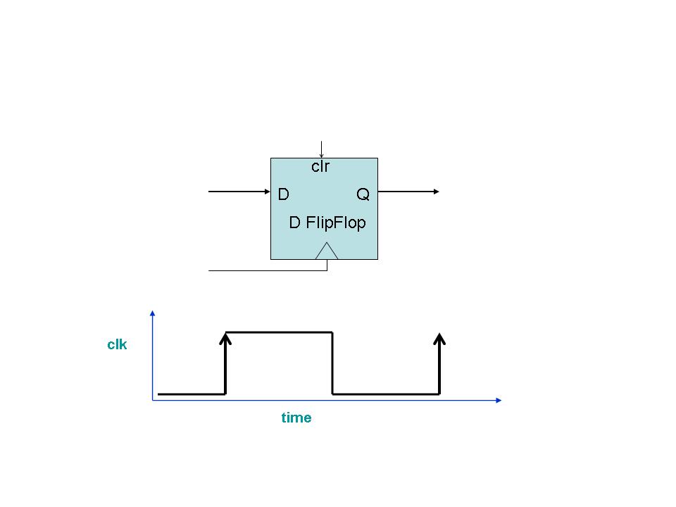
The figure below shows a sketch of the clock wave form and the flipflop we will be using. This is a positive edge triggered D flip flop. In addition to the clock input, it has a data input D. It holds a single bit of state, which is visible on its output Q. On the rising edge of the clock it captures D and stores it internally. Any other time, you can wiggle the input all you like, it won't change the output. In our synchronous design methodology, we make sure that all the inputs are stable before the edge arrives (remember, the clock cycle is longer than the delay along the critical path). Often a flipflop will have asynchronous inputs as well to clear or set the internal value.
In this class, we won't actually see how to construct flipflips from transistors ro gates. There is an art to it and you can study it in 150 if you like. Instead, we are going to use built-in elements.
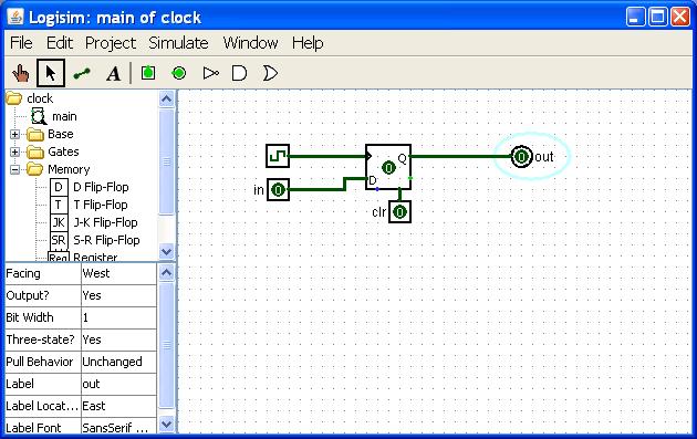
In Logisim, start a new project. Go to Project->Load Library->Built-in Library and select Memory. Opening this up you will see a D Flip-Flop. Add one to your empty schematic. Mouse over its pins so you can see its connections. You can read about it under Help. Connect an input pin to D and an output pin to Q. Under Base you will find a special pin called Clock. Drop it in and connect it to clock. It should look something like the following. Go ahead and open a logging window. Poke at D and see that nothing changes. You can poke clock, but Logsim has special support for the clock. Pull down the Simulate memu. You will see an option to tick once and also option to set the frequency and to start the clock running.
This circuit is the about the simplest example of our synchronous design methodology. Pretty much the whole circuit consists of a cycle containing one D flipflop and one inverter. (Incidently, the thing you just created is called a T flipflop. It toggles every clock tick.)
Given that your circuit has no input, you might wonder how do you initialize. If you go to Simulate->Reset Simulation you will see that the whole circuit goes undefined. When you tick the clock it sorts itself out. A better way to do this is to introduce an explicit reset. The Logsim D flipflop built-in has two asynchronous inputs - one to set it and one to clear it. Both ignore the clock. Attach a pin to the clear input. With this set to 1 you can let the clock tick away and the out value will be held to 0. When you release the clear it will start to toggle on the clock. The clear can be asserted at any time and it will reset the flipflop, even of the clock is not ticking.
Notice that every time the clock ticks, all state elements capture their new input simultaneously. Thus the new state is a function of the old state. When we put a collection of flipsflops together like this with a common set of control and clock inputs so that they function as a sngle unit, we call it a register. Here you have built a 4-bit register. With the adder it is a 4-bit counter.
Modify your circuit so that the constant input comes from a set of input pins, rather than the value 0001. Now you have a "by-N counter". At each clock tick, the new state is purely a function of the old state and the input pins.
In this case, the output of the circuit is exactly the state. Grab you old majority circuit that you built last week and attach it to the four output of the state regsiter to your majority circuit. Now you have a nice logic tester. If you put the state bits and the majority output into the logging tool let the clock tick to cycle through 0 - 15, the result should look exactly like your old truth table.
What you have built here is a finite state machine. In fact it is called a Moore machine. The new state is a function of the state and the inputs. The output is a function of the state. You could describe its behavior with a bubble-and-arc diagram. This machine implements a particular kind of state machine that just counts in a circle. The orbit depends on what you count by.
0000
1000
1100
1110
1111
0111
0011
0001
For extra credit, you can attach LEDS and buttons to your circuit from the built-in input-output library.