The design of digital systems is a classic example of "divide and conquer". We divide the problem into two simpler problmes: datapath and control. The datapath consists of registers, function units, and busses that connect outputs to inputs. The datapath has to be able to support the registers transfers and operations required to implement the design. But it does not have any of the intelligence. It does not know which register transfers to do when. It has a bunch of control inputs that tell it what to do. It is a puppet and the control points are the strings. It also has some outputs, called signals, that indicate when certain important events occur.
The other piece of the solutions is the controller. It's whole job is to figure out what registers transfers to do when and to assert the control points that cause these register transfers to be carried out. The controller is essentially a finite state machine. It has a control state. Its inputs are the signals from the datapath and its outputs are the control points.
We will gain more experience with these concepts of datapath and control over this and the next couple of labs as we move toward implementing a complete processor. The controllers for instruction interpretation are highly specialized.
Add a subcircuit called reg16. In this we'll create a 16-bit register with synchronous parallel load and asynchronous clear. Focus on reg16. Expand Memory and click on the register element. Its only attribute is bit width. Make it 16. Add a register to your reg16 circuit. Mouse over its pins. Like the D flipdlop it has a data input D, a data output Q, an asynchronous clr, and a clock. Every cycle this will capture whatever is on D, store it internally, and drive it on the outputs for the entire clock period.
Often we want to have lots of registers around to hold values, and we decide when to load a new value into each register. We'll create a subcircuit that reflects that concept. This is also the time to establish the "coding conventions" for our modules - for example, data inputs on the left, data outputs on the right, and control on the top. This will let us build datapaths that run left to right, like in the book. Logisim treats the clock specially. It has a special element type and you can tick it manually or automatically. We will wire the clock signal locally in the subcircuit; this will save us a lot of routing clock wires and ensures that it is handled consistently. You never never gate the clock. It just ticks. Selective loading of registers and the like is determined by the control signals.
To provide the parallel load capbility in your register subcircuit, place a MUX on the input and bring the output back to the 0 input of the mux. The 16-bit external input pin connects to the other input. The selector is your LOAD control signal. You'll need an input pin for clr and a 16-bit output. Now we have a register subcircuit with selective load. Place it in your main schematic and verify its behavior.
Notice, you can poke at individual bits in a multi-bit input pin. Notice also that the internal value of a register shows in its base symbol, but not when it is an element in a subcircuit. The way to gain visibility in the enclosing circuit when the output is not brought out to a pin is to attach a probe to the register subcircuit output. You will use this a lot in your project 4.
ld  dec
0    0  - hold value in register
0    1  - if (reg != 0) reg = reg - 1
1    x  - reg = In
You should be able to assert ld, tick the clock a full cycle (two ctrl-T), deassert ld and assert dec, and then watch it decrement down to zero as you tick the clock.
To build this, first, we dropped in a decrementer, connect a 16-bit input pin to In, a 16-bit output pin to Out, and and LED to zero. To make sure it all works, we put a pin on the Ld and Dec lines. Assert Ld. Step the clock twice (the rising edge and the falling edge). Unassert Ld and assert Dec. Step the clock till it reaches zero and the LED goes on. OK, this manual control is what we want to automate by building a control state machine. Before we do that, let's capture an real world input.
In Logisim's Input/Output library there is a button element. Drop one in your design and put a probe on the output. You'll see that it is 1 only while you hold it down. We'd like to use such a button to start our timer. The problem is that you might push it for an instant that does not quite include any clock edge. The way our state elements work is they sample their inputs right on the rising edge of the clock. We'll clean up the button by using a synchronizer. Drop a D flipflop in the design and connect the button to the asynchronous set pin (the left pin on the lower edge). This will cause the FF to be set to 1 when the button is pushed. Connect the constant 0 to the D input and connect the clock to the clock input. The output of the FF is a synchronized version of the button. Whenever you press the button it will go 1 until the next clock edge - just long enough for other parts of the circuit to use the signal.
Now we are ready to build a FSM controller to make the decrementer behave like a timer. Informally, when the button is pressed it should load the duration value and then it should count down till it reaches zero and turns on the LED.
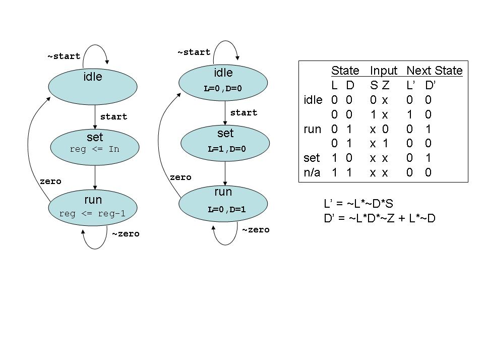
Designing a state machine is a stylized process. First we construct a symbolic state transition diagram (STD). This is a high level bubble and arc graph like you saw in your discrete math course. Each bubble represents a state. Inside the bubble we write down the register transfer that are to occur in that state. On the clock tick the specified register transfers is performed and transition to the next state occurs based on the inputs. We indicate the input by labeling the arcs with the input expression that causes that transition. The leftmost diagram below shows the symbolic STG for our timer.
The next stage in the FSM design process is the lower the symbolic STG by assigning a representation to the states and converting the register transfers to the control signals that will affect those transfers. Here we have made those two things the same. We have three states, so we need two state bits. We'll call them L and D. So 'idle' is 00, 'run' is 01, and set is '10'. In 'set' we assert L and deassert D, so the output that causes reg <= In is identical to the state bits. (Isn't that handy?)
The final stage is to convert the concrete STD to a truth table and generate logic that computes the state bits. Look carefully at the from of the truth table. The input columns are the current state and the 'inputs'. (X is a don't care. It is a convenient way to summarize multiple rows.) The output columns are the new state bits. When the clock ticks the new state bits will be loaded into to state FFs, thus advancing the state. Finally, we make sure that if the machine were to happen to be powered up in an illegal state (here 11) it would do something reasonable (here go to the idle state).
In timer.circ you have the classic form of a "Moore" FSM.
acc = acc + reg;as well as
reg = reg + 1;
To check the correctness of your solution you can verify that the result is equal to the sum of an arithmetic series. (Remember (A(1) + A(n))*n/2)
We have met several important abstractions in this class, including the instruction set abstraction at the hardware/software boundary and the digital abstraction at the logic gate. Here we meet the memory abstraction. A memory has two operations, read and write. We write a data value at an address. When we read an addres we get the most recent value written to that address.
A memory element has an address bus, a data bus, and some control signals. The width of the data is the unit of information that is read or written. The number of words that can be address with n bits is 2^n.
Actual memory chips have a specific height and width and number of data lines and address lines, etc.. And they come with a variety of different of using the control signals for performing operations. In Logisim we can pick the size of memory we want. And it is a "synchronous write, asynchronous read" protocol. We'll explain this as we go.
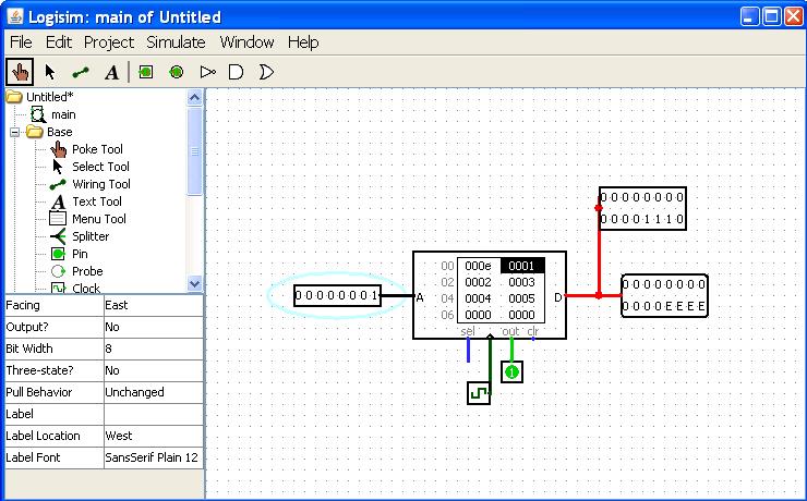
Create a new project and add the memory built-in library to it. Open up the memory library and click on RAM. The attributes gie you the opportunity to size the memory. Make the data bit width 16 bits and the address bit width 8. (How many bytes are in this memory?) Drop it in our schematic. Notice, there is only one set of data lines for reading and writing. A single wire can only be used for one thing at a time, so we will need to take turns.
Connect input pins of the proper width to A and out. You can connect a 1 to sel. We will focus first on reading, so put an output pin on the D line. Memories are used to hold lots of information. In Logsim we can initialize the contents of the memory. Right click the memory and select Edit Contents. Put some recongizable values in the various addresses. (You will notice that you can also save to a file or load from a file. We'll use this later.)
Assert out. Now the memory acts like a superduper combinational gate. The input is the address and the output is the contents of the memory at that address. Poke the address bits to select different addresses and check that the corresponding contents appear on D. We are reading it continuously.
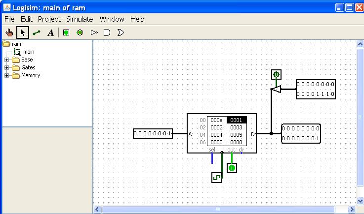
Poke the out to 0. Notice, the D lines all read x. This is not "don't care", this x is "undefined". The RAM is no longer driving any value on those lines. In order for something else to write the RAM, it needs to treat D as an input, not an output. Add a input pin to the D line (you may need to extend the wire as a T). Add a clock to the clk input with a wire so that you can see when the clock is high or low. Poke your new data input to be something different than the contents of the currently selected address. (Notice, not the input pins are driving the D line and the output pins on that line follow along.) Click the clock. On the rising edge the D value is written to the selected address. Click the clock again to complete the cycle. Play with this some more changing the address and the value and writing various words.
Now we are going to cause some trouble. Assert out. Look what happens to D. The orange indicates that two different sources are trying to drive the same wire. What value is on the wire? If it happens that they both drive low it will be a zero, or both high a one. What if one low and the other high? Logisim indicates this the the bit as E for ERROR as shown below. In the real hardware bad things happen and things get hot. Don't let this happen.
How is the accumulator similar or different from $1 in your MIPS machine?
We'll build a scaled down register file. Create a project that has your reg16 subcircuit in it. Drop eight of these down in the schematic. Add an 16-bit input Din and connect it to all the D inputs. This gives us a way to potentially write any register. To read one we need so select the one to read. Bring all eight Q outputs to a 16-bit wide 8-to-1 MUX with 3 selector inputs. Connect the selector to an input called A and drop an output pin on the output of the Mux called Dout. Now we have a small RAM. We can read any of the registers just by changing the address bits. How do we write just one? Drop in a decoder with 3 select bits and 8 outputs. Connect one to the Ld control for each register. You could connect the two sets of address lines together or you could keep them separate (like Rd and Rs). It's like a memory but smaller and simpler. None of the read/write handshake. You can read any register and write any register simultaneously. Try it out and make sure it works.
Any idea how you would make R0 read as zero? What would you do if you didn't want to write any register during some cycle?
fib' = temp + fib;
temp' = fib;
fib = fib'
temp = temp'
In your machine it is just two simultaneous register transfers. After N of these it stops.
Draw the state transition diagram with the register transfers and control signals. Turn in your solution as fib.circ along with two from the previous homework.