This week we will bring together
You will want to have your copy of P&H handy. The first three sections of chapter 5 introduce the concepts involved in implementing instructions from the top down. You should at least scan through those before starting the lab materials. If you look at Figure 5.1, you will notice that we saw most of the parts last week. It has instruction and data memories that are essentially the RAM we used. The PC and associated adders is similar to the incrementor. There is a register file and an ALU. We've got a bit more work to do to make a real machine out of these. To see where we are going, Figure 5.17 in P&H provides a road map for our coverage.
We'll start with the Arithmetic and Logic Unit (the ALU). This unit implements arithmetic and logic operations, as the name suggests:
In addition to the main ALU, there are three "mini-ALUs": one to add 4 to the program counter, another to compute a branch address, and the third to shift the contents of a branch immediate field.
The adder is given two 32-bit integers as inputs, and produces the sum as output.
You have already seen how one might go about designing an adder. Here's a quick review. Examining the truth table seems fruitless—there are 264 rows! Instead, we look for a way to break the problem down into smaller circuits that can be combined into the circuit we want. The standard addition-by-hand algorithm we learned in grade school provides a hint for how to do this.
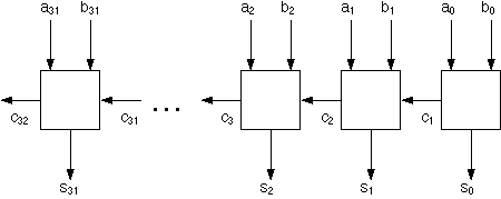
Consider, for example, the addition of two 4-bit values a and b, producing a sum s.
  a3 + a2 + a1 + a0
+ b3 + b2 + b1 + b0
------------------------
  s3 + s2 + s1 + s0
We start by adding the least significant bits, computing a0 + b0 = s0. A second output will represent a potential carry into column 1; we'll call that c1. Here's the truth table.
| a0 b0 | s0 c1 |
| 0 0 | 0 0 |
| 0 1 | 1 0 |
| 1 0 | 1 0 |
| 1 1 | 0 1 |
Adding in the second column from the right requires slightly different behavior, namely the use of an extra input—the carry from the first column. Here's its truth table.
| a1 b1 c1 | s1 c2 |
| 0 0 0 | 0 0 |
| 0 0 1 | 1 0 |
| 0 1 0 | 1 0 |
| 0 1 1 | 0 1 |
| 1 0 0 | 1 0 |
| 1 0 1 | 0 1 |
| 1 1 0 | 0 1 |
| 1 1 1 | 1 1 |
One may observe that the 1-bit adder just designed for the second addition column works for the remaining columns as well. That is, the same structure can be used to produce sk and ck+1 from ak, bk, and ck, for k ranging from 1 to 31. The resulting circuit is diagrammed below.
In fact, the addition in the rightmost column need not be treated as a special case. The adders used for columns 1-31 can also be used in column 0, merely by providing an input of 0 as the carry-in.
This circuit is called a ripple adder, since carries "ripple" from the rightmost to the leftmost columns. The possibility of a rippling carry constrains the speed of the adder. P&H section B.6 describes an adder design that trades simplicity for speed.
One of the very important properties of this adder is that it works for unsigned numbers and signed numbers (2's complement). In fact, it doesn't even need to know which kind it is working on—it does just the same thing in either case. Addition is moving clockwise on the number wheel. Plug in a positive and a negative 4-bit number in the 4-bit adder that you built last week. Convince yourself it does the right thing.
It is very useful to have the adder signal overflow when it occurs. This is one place where signed and unsigned arithmetic differs.
In adding unsigned values, detecting overflow is pretty obvious. If there is a carry out from the MSB there was an overflow. This is where you cross from FF...F to 00...0 on the number wheel.
The more interesting case is detecting overflow in addition of signed integers. If you add a positive and a negative number there cannot possibly be an overflow because the magnitude of A–B (for positive A and B) must be less than the larger of A and B.
When you add two positive signed values and an overflow occurs, there is no carry out. What happens instead?
Whenever you add two negative numbers there is a carry out since both have the sign bit on, so that is not what tells you there is an overflow. What does?
If you remember the number wheel, an overflow occurs when the result of the arithmetic operation crosses from the most positive numbers to the most negative, or vice versa. In other words, overflow occurs when adding two positive numbers produces a negative sum, or vice versa.
It is possible to detect the overflow using only the inputs and outputs of the most significant bit slice of your adder. Write down the truth table for the FA that forms the MSB of your adder. Add a 6th column that is overflow. Derive a boolean expression for the overflow. Can you reduce this to a single gate? Add this simple overflow detector to your 4-bit adder.
In designing our adder and in detecting overflow we reduced the mathematical concepts down to simple logic gates on the bits that are flowing along the wires. We can do a similar thing with subtraction. In your homework last week you designed a ripple subtractor. Here's another way to tackle the problem.
Recall, in 2's complement the value represented by a series of bits [Bn-1, Bn-2, ..., B0] is –Bn-12n-1 + Bn-22n-2 + ... + B0. Notice the minus sign associated with the numerical weight of the sign bit!
The arithmetic concept of negation, i.e. mapping A to –A, can be implemented on the bit representation by complementing all the bits (called the 1's complement and adding one to the result). (You can prove this rather easily.)
The operation A – B in two's complement arithmetic is equivalent to A + (~B) + 1. Thus we can use the adder for subtraction as well, by employing a multiplexor as shown below (and in your book).
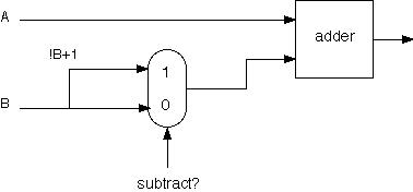
Negating all the bits in B is easy; we just route each bit through a NOT gate. Adding 1 to !B would seem to require an extra trip through the adder, but recall the design of the ripple adder. We had a carry-in input to the 1-bit adder for the least significant (rightmost) bit and we set it so 0. Instead, we could have done A + B + 1 with the same hardware. That's just what we need now. The diagram below shows how this is done.
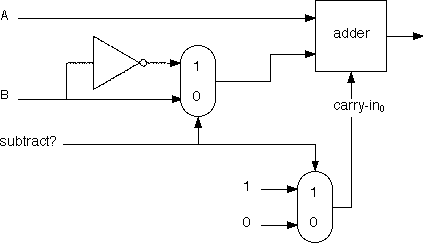
Modify your 4-bit adder so that it becomes an adder/subtractor. In addition to the two 4-bit data inputs A and B, it should have a one bit OP input. 0 means add, 1 means subtract. And while we are at it, let's make the design simpler and faster. All these inverters and muxes are nice, but a simple XOR gate will do the trick. Add one XOR gate to each bit slice (what was the FA) and one to the overall adder.
Congratulations, we are well along towards having an ALU. All we need to add is some logic.
Back in Lab 17 you implemented a logic unit that implemented four operations (AND, OR, XOR, and EQ) using gates and a MUX. How would you combine these this and your adder/subtractor into an "arithmetic logic unit".
What would the OP input be for this six-operation unit?
If you were to design the combined ALU as a bit slice, rather than by multiplexing two parallel units together, what additional savings in gates could be achieved?
Would you prefer to tackle the shifter as a bit slice or as a parallel unit?
We now move on to study the rest of the MIPS CPU, diagrammed in P&H Figure 5.17.
The diagram contains a lot of wires and four multiplexors. We'll examine these shortly. We've already studied parts of the ALU. The diagram includes several components that implement ALU parts: two other adders, a shifter, and a sign extender. There are two more combinational logic circuits labeled "Control" and "ALU control"; we'll examine these shortly as well. Finally, there are four state elements: the program counter, the registers, and two places to store input from memory or output to memory. One instruction per clock tick will be executed, and all the state elements will get updated at each clock tick.
The CPU in the diagram supports eight instructions. Three are I-format: beq, lw, and sw. Five are R-format: add, sub, and, or, and slt. (The j instruction is added last; the diagram for j appears in Figure 5.24.) Here is a review of the instruction formats for these instructions:
All the instructions start with an op code in bits 31-26.
The R-format instructions read two registers, specified in bits 25-21 and 20-16, and write into a third register, specified in bits 20-16.
There are two kinds of I-format instructions, beq and the two instructions referencing memory. Both kinds involve a signed immediate field in bits 15-0. The beq and sw instructions read values from registers specified in bits 25-21 and 20-16. The lw instruction reads from the register specified in bits 25-21, but writes to the register specified in bits 20-16.
The j instruction doesn't reference any registers. It computes an address from bits 25-0 of the instruction.
Execution of each instruction begins identically. The program counter signal goes to a state element that, given an address, retrieves the contents of memory at that address. The various bits of the instruction are routed to the "Control" module, which determines the functionality for each op code, and to the register state element, which selects register values relevant to the instruction.
We will deal later with fetching the instructions from memory and updating the PC. For today, we'll work with the 32-bit bus called Instruction in Figure 5.17 as an input. The first thing we do with an instruction is decode it so that we can determine how to execute it. In your project you have been doing this in software using shifts and masks. In hardware we do it by wiring and decode tables. You see this in Figure 5.17 using indices on the bits, such as instruction[31-26] for the OP field.
Start a new project called MIPS. Add an 32-bit wide input called Instruction. Use a splitter to crack it open into 32 individual values. Attach a 6-bit wide reverse splitter to bits 31-26 to create an output called OP. Do the same for the fields RS, RT, RD, Funct, and Immed. Notice that the last three overlap, i.e., they use the same bits of the instructions.
Some of these fields we will be able to use directly, others we will need to decode further.
In Figure 5-17 a 2-bit ALUOp signal that is derived from the 6-bit OP field and the 6-bit Funct field (which is referred to as the opcode field in the caption of the picture) are combined to produce the ALUop signal that specifies what ALU operation is to be performed. A table of signal values (Figure 5.12 in P&H) appears below.
| instruction | ALUOp | operation | function field | desired ALU action | ALU control input |
| lw | 00 | load word | don't care | add | 0010 |
| sw | 00 | store word | don't care | add | 0010 |
| beq | 01 | branch equal | don't care | subtract | 0110 |
| add | 10 | add | 100000 | add | 0010 |
| sub | 10 | subtract | 100010 | subtract | 0110 |
| and | 10 | and | 100100 | and | 0000 |
| or | 10 | or | 100101 | or | 0001 |
| slt | 10 | set on less than | 101010 | set on less than | 0111 |
Observe that the ALUOp signal specifies whether or not to use the funct field to direct the ALU; 10 means yes, 00 and 01 mean no. A truth table that derives ALU control values from the funct field values appears in Figure 5.13 of P&H.
You have probably noticed that there are two ways to derive the encoding of the control signals—starting from the encodings of the instruction fields and working towards the actual function units, or starting from the implementation of the function units. In practice, a combination is used. You probably noticed in your ALU design above that it really didn't matter which operators when to which inputs of the multiplexor. You might as well wire it up so that you can essentially use the bits from the instruction to make the selection.
The processor's 32 general-purpose registers are stored in a structure called a register file. The register file is a collection of registers in which any register can be read or written by specifying the number of the register in the file. As you saw in the last lab, a decoder is used to turn each 5-bit register field of an instruction into the corresponding register selector, and then the data in the corresponding register is output for use, say, by the ALU. Here's an example:
10100 => 20 => 32-bit contents of register 20
The register file for the MIPS uses three ports, two for reading and one for writing. The RS field is always used to select the register to be read on port 1. The data value is output on Read Data 1. Thus, bits [25-21] can be wired directly to Read Register 1. Similarly, the RT field is always used for Read Register 2 and the corresponding value is available at Read Data 2. Finally, the write register sometimes specified by RD (as in a R-type instruction) and sometimes by RT (as in an I-type) instruction.
P&H note (in Figure 5.7) the need to coordinate the reading of a register's value with the replacement of the value in that register. During what portion of the cycle are the read values used and when is the write value utilized? What happens if the read register and the write register happen to be the same?
How would you determine whether the instruction is an R-type or I-type?
Let's build a little extender in Logisim. We'll scale it down a bit from the MIPS. It should have a 8 bit data input In, a control input X (0 => zero extend, 1=> sign extend) and a 16-bit data output, Out. It is mostly splitters, but you'll need a little logic to select the bit.
The meaning of each instruction is defined by the register transfers that take place when it is executed. These transfers are carried out by the data path. So, to determine what needs to be connected to what, we write down all the register transfers that we need to do. Then we makes sure that we can do them all. Finally, when we design the control logic so that the control signals cause the right ones to take place.
Look back at the subset of instructions that are in the ALU control table above. What is the register transfer required for the R-type instructions—add, sub, and, or, slt? They all have the form R[rd] = R[rs] op R[rt].
| instruction | operation | Register Transfer |
| lw | load word | |
| sw | store word | |
| beq | branch equal | |
| add | add | R[rd] = R[rs] + R[rt] |
| sub | subtract | R[rd] = R[rs] - R[rt] |
| and | and | R[rd] = R[rs] & R[rt] |
| or | or | R[rd] = R[rs] | R[rt] |
| slt | set less than | R[rd] = R[rs] < R[rt] |
| instruction | operation | Register Transfer |
| lw | load word | R[rt]=Mem[ R[rs]+SX(im16) ]; PC = PC+4 |
| sw | store word | Mem[ R[rs]+SX(im16) ] = R[rt]; PC = PC+4 |
| beq | branch equal | PC = R[rs] == R[rt] ? PC+4 + SX(im16) : PC+4 |
| add | add | R[rd] = R[rs] + R[rt]; PC = PC+4 |
| sub | subtract | R[rd] = R[rs] - R[rt]; PC = PC+4 |
| and | and | R[rd] = R[rs] & R[rt]; PC = PC+4 |
| or | or | R[rd] = R[rs] | R[rt]; PC = PC+4 |
| slt | set less than | R[rd] = R[rs] < R[rt]; PC = PC+4 |
Now that we have verified that everything that needs to get somewhere has a way to get there, we need to determine how to set the various control signals to actually get them there. To do this, we add a column to our table for each control signal in the data path. (We'll let you do the PC mini ALU.) Most of these are MUX selectors. We just fill them in according to the RTL. (We've a symbolic version of the ALUop.) You should fill in the rest of the table.
| inst | operation | Register Transfer | SX | ALUSrc | ALU op | MemRead | MemToReg | MemWrite | RegWrite |
| lw | load word | R[rt]=Mem[ R[rs]+SX(im16) ]; PC = PC+4 | 1 | 1 | add | 1 | 1 | 0 | 1 |
| sw | store word | Mem[ R[rs]+SX(im16) ] = R[rt]; PC = PC+4 | |||||||
| beq | branch equal | PC = R[rs] == R[rt] ? PC+4 + SX(im16) : PC+4 | |||||||
| add | add | R[rd] = R[rs] + R[rt]; PC = PC+4 | x | 0 | add | 0 | 0 | 0 | 1 |
| sub | subtract | R[rd] = R[rs] - R[rt]; PC = PC+4 | |||||||
| and | and | R[rd] = R[rs] & R[rt]; PC = PC+4 | |||||||
| or | or | R[rd] = R[rs] | R[rt]; PC = PC+4 | |||||||
| slt | set less than | R[rd] = R[rs] < R[rt]; PC = PC+4 |
The lw instruction has op code = 0x23, source register in bits 25-21, destination register in bits 20-16, and offset in bits 15-0. The Branch and MemWrite signals are 0; the MemRead signal is 1.
What's the value of the MemtoReg signal?
What's the value of the RegDst signal?
What's the value of the RegWrite signal?
What's the value of the ALUSrc signal?
Explain the processing of the beq instruction, in the upper right corner of Figure 5.17. In particular, explain the purpose of the AND gate, and why an ALU output of "zero" might be relevant.
A common bug in circuitry is for a wire to be always "on". What would be the effect of having the ALUSrc wire always on? In particular, which instructions would no longer work correctly? Redundant Signal Critical Path
The MIPS CPU in P&H Figure 5.17 implements eight instructions. It is obviously incomplete. However, almost all the missing instructions can make use of the existing structure. To implement a new instruction, we first identify the functional units—register file, ALU, PC, or memory—needed by the instruction. There must be data paths along which information can access these functional units. We then choose existing control signals, perhaps with extra gates, or add new control signals that route information appropriately. (The meaning of the control signals produced by the Control and the ALU control logic is given here.)
As an example, we implement the addi (Add Immediate) instruction. Its op code is 0x8; it replaces the value in register rt by the sum of the sign-extended immediate field and the value in register rs. Its processing is likely to be similar to that of add; we will use this information as a self-check once we complete the addi implementation.
First, we fill in the values for existing control signals.
RegDst = 0 since the result should be stored in register rt.
RegWrite = 1 since a register's value is getting replaced.
ALUSrc = 1 since the second ALU operand is coming from the instruction's immediate field.
Branch = MemRead = MemWrite = MemtoReg = 0 since the instruction isn't a branch and doesn't access memory.
ALUOp requires more consideration. The ALUOp value for add (10) would seem to be appropriate, but the ALU control logic then proceeds to determine the ALU operation from the funct field of the instruction. For now, we can get the desired behavior from assigning ALUOp = 00—that is, by mimicking the ALU behavior of lw and sw—but in general we will need an extra ALUOp bit that says to use or ignore the funct field.
Comparing this to the control signals for add yields no surprises.
| signal | add | addi |
| RegDst | 1 | 0 |
| RegWrite | 1 | 1 |
| ALUSrc | 0 | 1 |
| Branch | 0 | 0 |
| MemRead | 0 | 0 |
| MemWrite | 0 | 0 |
| MemtoReg | 0 | 0 |
| ALUOp | 10 | 00 |
We move to the j (Jump) instruction. Adding it to the instruction set requires a different approach, since it uses neither registers nor the ALU nor memory access. Its sole effect on the CPU's state elements is to change the PC. (Recall that the new PC address is the concatenation of the top four bits of the current PC+4, bits 25-0 of the instruction, and 00.
Figure 5.24 shows what's needed:
shift-left-2 logic, and a wire supplying bits 25-0 of the instruction to the shifter;
logic to concatenate the top four bits of PC+4 to the shifted address;
a new control signal named "Jump", and a multiplexor that uses Jump to select either the computed branch address or the jump address as the new PC.
The new wires and logic appear in solid black in Figure 5.24.
(Self Test)RegDst and RegWrite for oriWe'll continue exploring the CPU next lab. Read sections 5.1 through 5.4 in P&H for background.