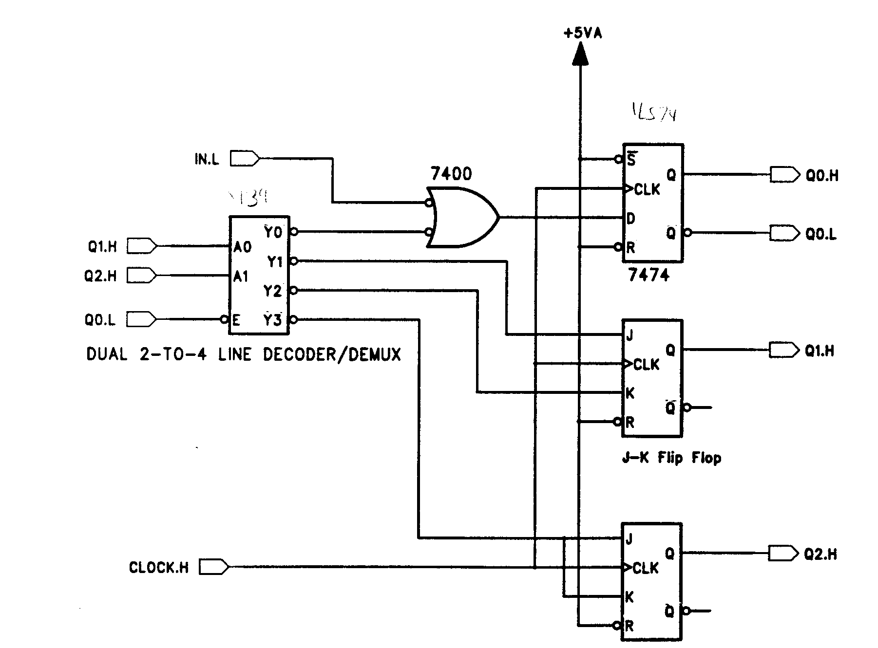
2. Sequential Circuits (20 pts)
a. For the circuit shown, complete the state transition table
below: (16 pts)
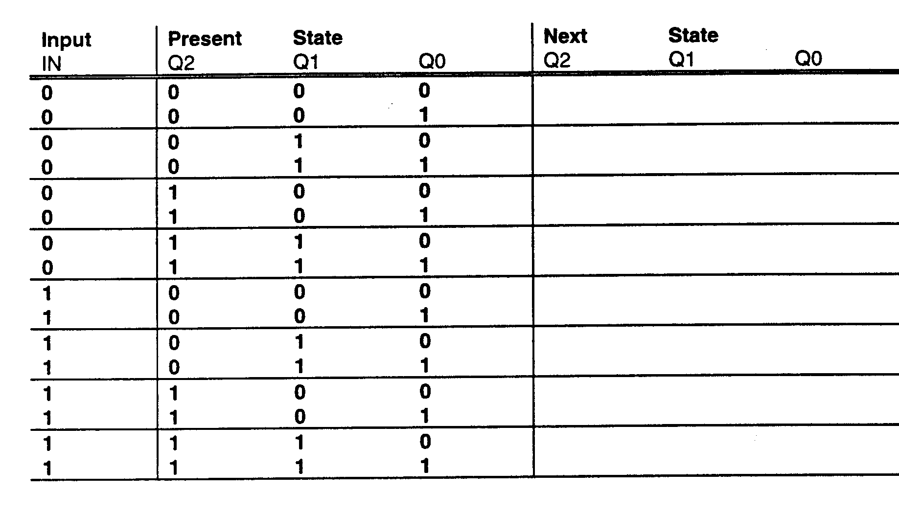
b. Which states (Q2A1Q0) are unreachable? (4 pts)
Problem 5 is just for the fun of it, itis not covered on our quiz 1.
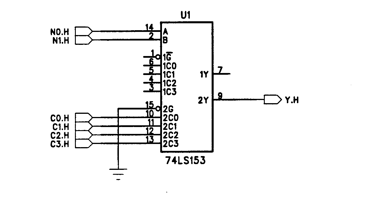
5. Implement Y (N3, N2, N1, N0) = Sigma(m0, m3, m5, m6, m7, m9, m10,
m12, m14, m15) using one section of a 74153 dual 4:1 mux and minimum extra
gates. (10 pts)
Write equations for C0, C1, C2, and C3:
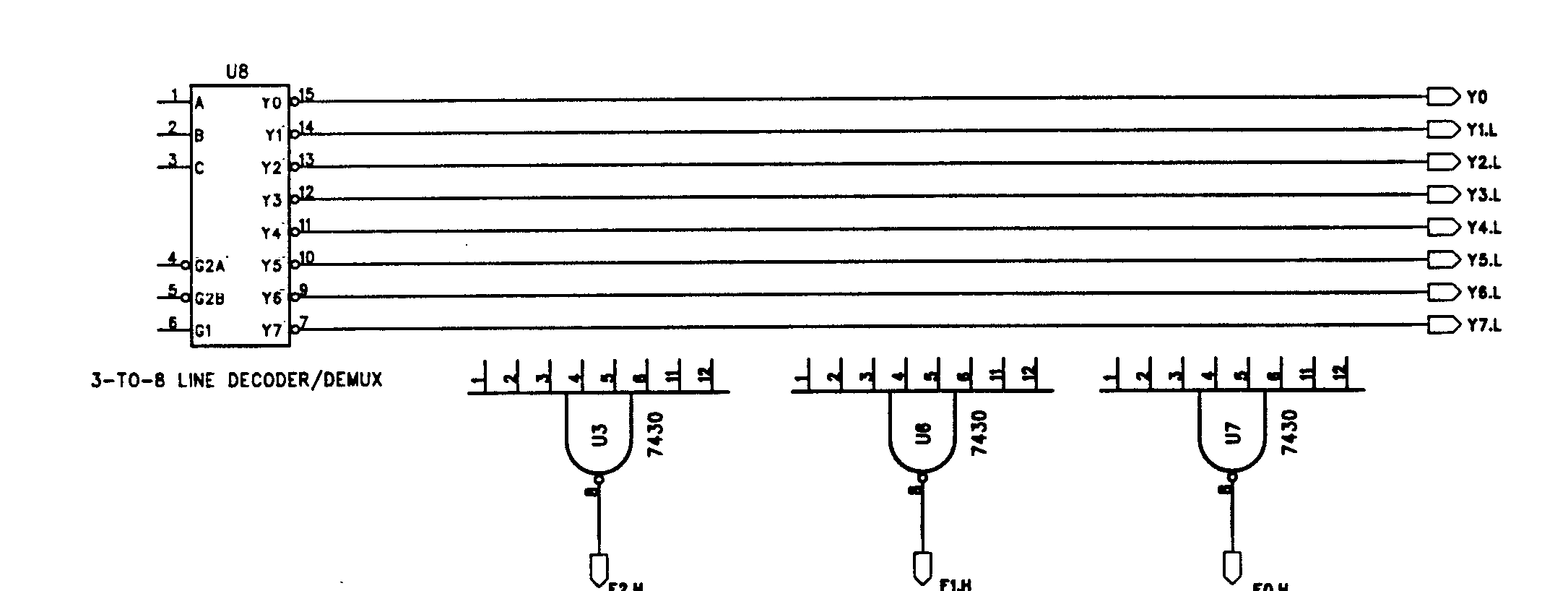
Problem 6 is just for the fun of it, it is not covered on our quiz 1.
6. Complete the design of the circuit below so that it functions
as a 3 bit add-one circuit. A 3 bit number X=[X2X1X0] is input, and
the output F = [F2F1F0] should be equal to X+1. For example, if the
input is [0 1 1] the output should be [1 0 0], i.e. F2=1, F1=0, and
F0=0. You should not need to add any extra gates. (10 pts)