Project 3.1 CPU - ALU and Regfile
Deadline: 11:59 PM, Wednesday November 6th
Getting started
Please accept the Github classroom assignment by clicking this link. Once you’ve created your repository, you’ll need to clone it on the machine you’ll be working on. For Logisim assignments, we recommend that you work on your local machine, or that you physically come to Soda and work on the lab computers in 271, 273, 275, 277, or 330 Soda.
Logisim is a Java program that requires a GUI, so you won’t be able to work remotely on the lab computers without using window forwarding. We highly recommend that you do not use window forwarding. If you’re using your local machine, make sure you have Java installed. If you use WSL for CS 61C assignments, don’t work from WSL; instead, work from your Windows OS.
You’ll also need to add the staff starter repo as a remote using this command:
$ git remote add staff https://github.com/61c-teach/fa19-proj3-starter.git
If we publish changes to the starter code, you can get them by running git pull staff master
This project will be comleted in the digital logic simulation software Logisim Evolution.
IMPORTANT: Please use the .jar file we’ve given you, not the version of Logisim that is downloaded on the lab computers! And a note: Logisim does not save your work as you go along, and it does not automatically create a new .circ file when you open it! Save when you start, and save frequently as you work.
You can open Logisim using the following command:
$ java -jar logisim-evolution.jar
You can also directly open the jar file, then click File -> Open on the menu bar.
Important Information: Please Read!
- You are allowed to use any of Logisim’s built-in blocks for all parts of this project.
- Save frequently and commit frequently! Try to save your code in Logisim every 5 minutes or so, and commit every time you produce a new feature, even if it is small.
- Tests for a completed ALU, RegFile and
addiinstruction have been included with the project starter code. You can run them with the commandsalu-test.sh,./reg-test.sh,cpu-part1-single.sh, andcpu-part1-pipelined.sh. See the Testing section for information on how to interpret your test output. The final submission for the project will be through Gradescope, but the tests will be exactly the same as those that are run with the four testing shell scripts. - Don’t move around the given inputs and outputs in your circuit; this could lead to issues with the autograder.
- Because the files you are working on are actually XML files, they’re quite difficult to merge properly. Do not work on the project in two places and attempt to merge your changes! We highly recommend that if you’re working with a partner, you sit together and pair program this assignment.
Exercise 1: Arithmetic Logic Unit (ALU)
Your first task is to create an ALU that supports all the operations needed by the instructions in our ISA (which is described in further detail in the next section). Please note that we treat overflow as RISC-V does with unsigned instructions, meaning that we ignore overflow.
We have provided a skeleton of an ALU for you in alu.circ. It has three
inputs:
| Input Name | Bit Width | Description |
|---|---|---|
| A | 32 | Data to use for Input A in the ALU operation |
| B | 32 | Data to use for Input B in the ALU operation |
| ALUSel | 4 | Selects which operation the ALU should perform (see the list of operations with corresponding switch values below) |
… and one output:
| Output Name | Bit Width | Description |
|---|---|---|
| Result | 32 | Result of the ALU operation |
Below is the list of ALU operations for you to implement, along with their associated ALUSel values. All of them are required with the exception of mulh, which will take some extra effort to implement (but you’re certainly up to the task!). You are allowed and encouraged to use built-in Logisim blocks to implement the arithmetic operations.
| Switch Value | Instruction |
|---|---|
| 0 | add: Result = A + B |
| 1 | and: Result = A & B |
| 2 | or: Result = A | B |
| 3 | xor: Result = A ^ B |
| 4 | srl: Result = (unsigned) A >> B |
| 5 | sra: Result = (signed) A >> B |
| 6 | sll: Result = A << B |
| 7 | slt: Result = (A < B (signed)) ? 1 : 0 |
| 8 | divu: Result = (unsigned) A / B |
| 9 | remu: Result = (unsigned) A % B |
| 10 | mul: Result = (signed) (A * B)[31:0] |
| 11 | mulhu: Result = (A * B)[63:32] |
| 12 | sub: Result = A - B |
| 13 | bsel: Result = B |
| 14 | mulh: Result = (signed) (A * B)[63:32] |
When implementing mul and mulh, notice that the multiply block has a “Carry Out” output (the adder block also has this, but you will not need this) located here:
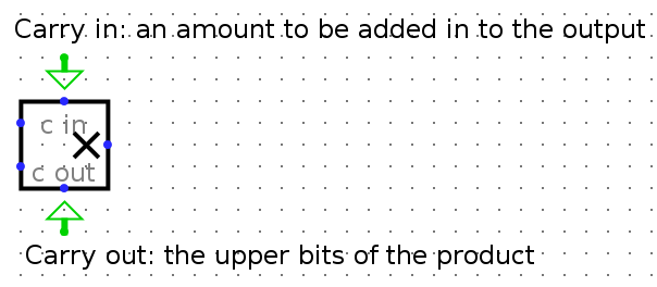
Experiment a bit with it, and see what you get for both the result and carryout with negative and positive 2’s complement numbers. You should realize why we made mulh extra credit.
Hints:
addis already made for you, and feel free to use a similar structure when implementing your other blocks.- You can hover your cursor over an output/input on a block to get more detailed information about that input/output.
- You might find bit splitters or extenders useful when implementing
sraandsrl. - Use tunnels! They will make your wiring cleaner and easier to follow, and will reduce your chances of encountering unexpected errors.
- A multiplexer (MUX) might be useful when deciding which block output you want to ouput. In other words, consider simply processing the input in all blocks, and then outputing the one of your choice.
NOTE: Your ALU must be able to fit in the provided harness alu_harness.circ. Follow the same instructions as the register file regarding rearranging inputs and outputs of the ALU. In particular, you should ensure that your ALU is correctly loaded by a fresh copy of alu_harness.circ before you submit.
ALU Testing
When you run ./alu-test.sh, the ALU tests will produce output in the part1-tests/alu-tests/student_output directory. We’ve provided a python script called binary_to_hex_alu.py that can interpret this output in a readable format for you. To use it, do the following: (you may have to use “py” or “python” as is appropriate on your machine)
$ cd tests
$ python3 binary_to_hex_alu.py PATH_TO_OUT_FILE
For example, to see reference_output/alu-add-ref.out in readable format, you would do this:
$ cd part1-tests/alu-tests
$ python3 binary_to_hex_alu.py reference_output/alu-add-ref.out
If you want to see the difference between your output and the reference solution, put the readable outputs into new .out files and diff them. For example, for the alu-add test, take the following steps:
$ cd part1-tests/alu-tests
$ python3 binary_to_hex_alu.py reference_output/alu-add-ref.out > alu-add-ref.out
$ python3 binary_to_hex_alu.py student_output/alu-add-student.out > alu-add-student.out
$ diff alu-add-ref.out alu-add-student.out
Exercise 2: Register File (RegFile)
As you learned in class, RISC-V architecture has 32 registers. However, in this project, You will only implement 9 of them (specified below) to save you some repetitive work. This means your rs1, rs2, and rd signals will still be 5-bit, but we will only test you on the specified registers.
Your RegFile should be able to write to or read from these registers specified in a given RISC-V instruction without affecting any other registers. There is one notable exception: your RegFile should NOT write to x0, even if an instruction try. Remember that the zero register should ALWAYS have the value 0x0. You should NOT gate the clock at any point in your RegFile: the clock signal should ALWAYS connect directly to the clock input of the registers without passing through ANY combinational logic.
The registers and their corresponding numbers are listed below.
| Register Number | Register Name |
|---|---|
| x0 | zero |
| x1 | ra |
| x2 | sp |
| x5 | t0 |
| x6 | t1 |
| x7 | t2 |
| x8 | s0 |
| x9 | s1 |
| x10 | a0 |
You are provided with the skeleton of a register file in regfile.circ. The register file circuit has six inputs:
| Input Name | Bit Width | Description |
|---|---|---|
| Clock | 1 | Input providing the clock. This signal can be sent into subcircuits or attached directly to the clock inputs of memory units in Logisim, but should not otherwise be gated (i.e., do not invert it, do not “and” it with anything, etc.). |
| RegWEn | 1 | Determines whether data is written to the register file on the next rising edge of the clock. |
| Read Register 1 (rs1) | 5 | Determines which register’s value is sent to the Read Data 1 output, see below. |
| Read Register 2 (rs2) | 5 | Determines which register’s value is sent to the Read Data 2 output, see below. |
| Write Register (rd) | 5 | Determines which register to set to the value of Write Data on the next rising edge of the clock, assuming that RegWEn is a 1. |
| Write Data (wb) | 32 | Determines what data to write to the register identified by the Write Register input on the next rising edge of the clock, assuming that RegWEn is 1. |
The register file also has the following outputs:
| Output Name | Bit Width | Description |
|---|---|---|
| rs1 | 32 | Driven with the value of the register identified by the Read Register 1 input. |
| rs2 | 32 | Driven with the value of the register identified by the Read Register 2 input. |
ra Value |
32 | Always driven with the value of ra (This is a DEBUG/TEST output.) |
sp Value |
32 | Always driven with the value of sp (This is a DEBUG/TEST output.) |
t0 Value |
32 | Always driven with the value of t0 (This is a DEBUG/TEST output.) |
t1 Value |
32 | Always driven with the value of t1 (This is a DEBUG/TEST output.) |
t2 Value |
32 | Always driven with the value of t2 (This is a DEBUG/TEST output.) |
s0 Value |
32 | Always driven with the value of s0 (This is a DEBUG/TEST output.) |
s1 Value |
32 | Always driven with the value of s1 (This is a DEBUG/TEST output.) |
a0 Value |
32 | Always driven with the value of a0 (This is a DEBUG/TEST output.) |
The test outputs at the top of your regfile.circ file are present for testing and debugging purposes. If you were implementing a real register file, you would omit those outputs. In our case, be sure they are included correctly–if they are not, you will not pass.
You can make any modifications to regfile.circ you want, but the outputs must obey the behavior specified above. In addition, your regfile.circ that you submit must fit into the regfile_harness.circ file we have provided for you. This means that you should take care not to move inputs or outputs. To verify changes you have made didn’t break anything, you can open regfile_harness.circ and ensure there are no errors and that the circuit functions well. (The tests use a slightly modified copy of regfile_harness.circ.)
Hints:
- Take advantage of copy-paste! It might be a good idea to make one register completely and use it as a template for the others to avoid repetitive work.
- I would advise you not to use the enable input on your MUXes. In fact, you can turn that feature off. I would also advise you to also turn “three-state?” to off. Take a look at all the inputs to a logisim register and see what they all do.
- Again, MUXes are your friend, but also DeMUXes.
- Think about what happens in the register file after a single instruction is executed. Which values change? Which values stay the same? Registers are clock-triggered–what does that mean?
- Keep in mind registers have an “enable” input available, as well as a clock input.
- What is the value of
x0?
RegFile Testing
When you run ./reg-test.sh, the RegFile tests will produce output in the part1-tests/reg-tests/student_output directory. We’ve provided a python script called binary_to_hex_regfile.py that can interpret this output in a readable format for you. To use it, do the following commands: (you may have to use “py” or “python3” as is appropriate on your machine)
$ cd part1-tests/reg-tests
$ python binary_to_hex_regfile.py PATH_TO_OUT_FILE
For example, to see reference_output/regfile-x0-ref.out in readable format, you would do this:
$ cd part1-tests/reg-tests
$ python binary_to_hex_regfile.py reference_output/regfile-x0-ref.out
If you want to see the difference between your output and the reference solution, put the readable outputs into new .out files and diff them. For example, for the regfile-x0 test, take the following steps:
$ cd part1-tests/reg-tests
$ python binary_to_hex_regfile.py reference_output/regfile-x0-ref.out > regfile-x0-ref.out
$ python binary_to_hex_regfile.py student_output/regfile-x0-student.out > regfile-x0-student.out
$ diff regfile-x0-ref.out regfile-x0-student.out
Exercise 3: Addi Instruction
As your final task for Part 1 of the project, you’re going to implement a CPU that’s capable of executing one instruction: addi! You’re welcome to implement other instructions at this time, but for Project 3-1, you’ll only be graded on whether or not addi executes correctly. When we release Project 3-2, there will be more detailed instructions on how to implement the other instructions.
1) Processor
We have provided a skeleton for your processor in cpu.circ. You will be using your own implementations of the ALU and RegFile as you construct your datapath. You are responsible for constructing the entire datapath from scratch. For 3.1, your completed processor should support the addi instruction using a two-stage pipeline, with IF in the first stage and ID, EX, MEM, and WB in the second stage. To start, however, we recommend you create a single-stage processor with no pipelining. Once that is working, you can modify your processor so that it has a 2-stage pipeline.
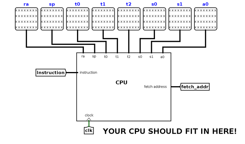
Your processor will get its program from the processor harness run.circ. Your processor will output the address of an instruction, and accept the instruction at that address as an input; essentially, it serves as instruction memory. We recommend that you take some time to inspect run.circ to see exactly what’s going on. (This same harness will be used to test your final submission, so make sure your CPU fits in the harness before submitting your work!) Your processor has 2 inputs that come from the harness:
| Input Name | Bit Width | Description |
|---|---|---|
| INSTRUCTION | 32 | Driven with the instruction at the instruction memory address identified by the FETCH_ADDRESS (see below). |
| CLOCK | 1 | The input for the clock. As with the register file, this can be sent into subcircuits (e.g. the CLK input for your register file) or attached directly to the clock inputs of memory units in Logisim, but should not otherwise be gated (i.e., do not invert it, do not AND it with anything, etc.). |
Your processor must provide the following outputs to the harness:
| Output Name | Bit Width | Description |
|---|---|---|
| ra | 32 | Driven with the contents of ra. FOR TESTING |
| sp | 32 | Driven with the contents of sp. FOR TESTING |
| t0 | 32 | Driven with the contents of t0. FOR TESTING |
| t1 | 32 | Driven with the contents of t1. FOR TESTING |
| t2 | 32 | Driven with the contents of t2. FOR TESTING |
| s0 | 32 | Driven with the contents of s0. FOR TESTING |
| s1 | 32 | Driven with the contents of s1. FOR TESTING |
| a0 | 32 | Driven with the contents of a0. FOR TESTING |
| fetch_addr | 32 | This output is used to select which instruction is presented to the processor on the INSTRUCTION input. |
Just like with the ALU and RegFile, be careful NOT to move the input or output pins! See the “Testing” section for more information on the harness and tests.
2) Memory
The memory unit is already fully implemented for you! For part1, the addi instruction does NOT use the Memory unit, you can leave it untouched for now.
If you are interested, here’s a quick summary of its inputs and outputs:
| Signal Name | Direction | Bit Width | Description |
|---|---|---|---|
| WriteAdd | Input | 32 | Address to read/write to in Memory |
| WriteData | Input | 32 | Value to be written to Memory |
| MemRW | Input | 1 | Equal to one on any instructions that write to Memory and zero otherwise |
| CLK | Input | 1 | Driven by the clock input to the CPU |
| ReadData | Output | 32 | Value of the data stored at the specified address |
3) Controls
Designing your control unit will probably be your biggest challenge in Project 3.2. For 3.1, you can put a constant for each control signal, because addi is the only instruction you’ll be implementing. As you implement addi, think about where you’ll need to make additions in order to support other instructions.
4) Getting Started: A Guide
We know that trying to build a CPU with a blank slate might be intimidating, so we wrote this guide to help you.
Recall the five stages of the CPU pipeline:
- Instruction Fetch
- Instruction Decode
- Execute
- Memory
- Write Back
This guide will help you work through each of these stages for the addi instruction. Each section will contain questions for you to think through and pointers to important details, but it won’t tell you exactly how to implement the instruction.
You may need to read and understand each question before going to the next one, and you can see the answers by clicking on the question. During your implementation, feel free to place things in subcircuits as you see fit.
Stage 1: Instruction Fetch
The main thing we are concerned about in this stage is: how do we get the current instruction? From lecture, we know that instructions are stored in the instruction memory, and each of these instructions can be accessed through an address.
1. Which file in the project holds your instruction memory? How does it connect to your cpu.circ file?
The instruction memory is the ROM module in `run.circ`. It provides an input into your CPU named `INSTRUCTION` and takes an output from your CPU. In your `cpu.circ` file, that output is called "PROGRAM_COUNTER". In `run.circ`, it is called `fetch_addr`.2. In your CPU, how would changing the address you output as `PROGRAM_COUNTER` affect the instruction input?
The instruction that `run.circ` outputs to your CPU should be the instruction at address `PROGRAM_COUNTER` (or `fetch_addr`) in instruction memory.3. How do you know what `PROGRAM_COUNTER` should be?
`PROGRAM_COUNTER` is the address of the current instruction being executed, so it is saved in the PC register. For this project, your PC will start at 0, as that is the default value for a register.4. For basic programs without any jumps or branches, how will the PC change from line to line?
The PC must increment by 1 instruction in order to go to the next instruction, as the address held by the PC register represents what instruction to execute. This means that your PC will increase by 4 (assuming no branch or jump) line to line.We have provided the PC register in the cpu.circ file. Please implement the PC’s behavior for simple programs - ignoring jumps and branches. You will implement branches and jumps in Part 2 of the project, but for now we are only concerned with being able to run addi instructions. Remember to connect the clock!
Remember that we will in the end implement a 2-stage pipelined processor, so the IF stage is separate from the remaining stages. What circuitry separates the different stages of a pipeline? Specifically, what circuitry separates IF from the next stage? Will you need to add anything?
Stage 2: Instruction Decode
Now that we have our instruction coming from the instruction input, we have break it down in the Instruction Decode step, according to the RISC-V instruction formats you have learned.
1. What type of instruction is addi? What are the different bit fields and which bits are needed for each?
I type. The fields are: - `imm [31-20]` - `rs1 [19-15]` - `funct3 [14-12]` - `rd [11-7]` - `opcode [6-0]`2. In Logisim, what tool would you use to split out different groups of bits?
Splitter!4. Now we need to get the data from the corresponding registers, using the register file. Which instruction fields should be connected to the register file? Which inputs of the register file should it connect to?
Instruction field `rs1` will need to connect to read register 1.6. What does the Immediate Generator need to do?
For addi, the immediate generator takes in 12 bits and produces a signed 32-bit immediate. We highly suggest you create an Immediate Generator subcircuit!Stage 3: Execute
The Execute stage is where the computation of most instructions is performed. This is also where we will introduce the idea of using a Control Module.
1. For the add instruction, what should be your inputs in to the ALU?
Read Data 1 (rs1) and the immediate produced by the Immediate Generator.2. In the ALU, what is the purpose of ALU_Sel?
It determines which operation the ALU will perform.3. Although it is possible for now to just put a constant as the ALUSel, why would this be infeasible as you need to implement more instructions?
With more instructions, the input to the ALU might need to change, so you will need to have some sort of circuit that changes ALUSel depending on the instruction being executed.Stage 4: Memory
The memory stage is where the memory can be written to using store instructions and read from using load instructions. Because the addi instruction does not use memory, we will not spend too much time here.
Bring in the MEM module that we provided. At this point, we cannot connect most of the inputs, as we don’t know where they should come from. However, you can still connect the clock.
Stage 5: Write back
The write back stage is where the results of the operation is saved back to the registers.
1. Do `addi` instruction need to write back to a register?
Yes. `addi` takes the output of a an addition computation in the ALU and writes it back to the register file.3. What should you use as the Select input to the MUX? What does the input depend on?
This input should be able to choose between three MUX inputs: (1) ALU, (2) MEM, and (3) PC + 4 (when will you use this?) The control signal that determines which of these inputs is written back is called WBSel. For now, there should only be one value that WBSel can take on -- whatever it should be for `addi`.4. Now that we have the inputs to the MUX sorted out, we need to wire the output. Where should the output connect to?
Because the output is the data that you want to write into the Register File, it should connect to the Write Data input on the Register File.If you have done all of the following steps correctly, you should have a single-cycle processor that works for addi instructions.
Run ./cpu-part1-single.sh and see if it’s working correctly!
5) Pipelining
1. Instruction Fetch: An instruction is fetched from the instruction memory.
2. Execute: The instruction is decoded, executed, and committed (written back). This is a combination of the remaining four stages of a normal five-stage RISC-V pipeline (ID, EX, MEM and WB).
Because all of the control and execution is handled in the Execute stage, your processor should be more or less indistinguishable from a single-cycle implementation, barring the one-cycle startup latency. However, we will be enforcing the two-stage pipeline design. Some things to consider:
- Will the IF and EX stages have the same or different
PCvalues? - Do you need to store the
PCbetween the pipelining stages?
You might also notice a bootstrapping problem here: during the first cycle, the instruction register sitting between the pipeline stages won’t contain an instruction loaded from memory. How do we deal with this? It happens that Logisim automatically sets registers to zero on reset; the instruction register will then contain a nop. We will allow you to depend on this behavior of Logisim. Remember to go to Simulate --> Reset Simulation (Ctrl+R) to reset your processor.
After pipelining your processor, you should be able to pass ./cpu-part1-pipelined.sh test.
Testing
Understanding how the tests work
Each test is a copy of the run.circ file included with the starter code that has instructions loaded into its IMEM. When you run logisim-evolution from the command line, the clock ticks, the program counter is incremented, and the values in each of the outputs is printed to stdout.
Let’s take as the one stage addi test as an example. It has 3 addi instructions (addi t0, x0, 5, addi t1, t0, 7, addi s0, t0, 9).
If you open onestage-tests/circ_files/CPU_addi.circ in Logisim Evolution, it’ll look like this:
Let’s take a closer look at the various parts of the test file. At the top, you’ll see the place where your CPU is connected to the test outputs. With the skeleton file, you’ll see all xxxx’s, as you do below; when your CPU is working, this should not be the case. Your CPU takes in one input (instruction), and along with the values in each of the registers, it has one additional output: fetch_addr, or the address of the instruction to be fetched from IMEM to be executed the next clock cycle.
Be careful that you don’t move any of the inputs/outputs of your CPU around, or add any additional inputs/outputs. This will change the shape of the CPU subcircuit, and as a result the connections in the test files may no longer work properly.
Below the CPU, you’ll see instruction memory. The hex for the 3 addi instructions (0x00500293, 0x00728313, 0x00928413) has been loaded into instruction memory. Instruction memory takes in one input (called fetch_addr) and outputs the instruction at that address. fetch_addr is a 32-bit value, but because Logisim Evolution caps the size of ROM units at 2^16B, we have to use a splitter to get only 14 bits from fetch_addr (ignoring the bottommost two bits). Notice that fetch_addr is a byte address, not a word address.
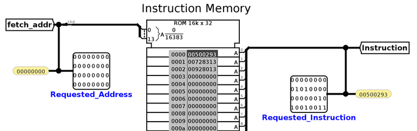
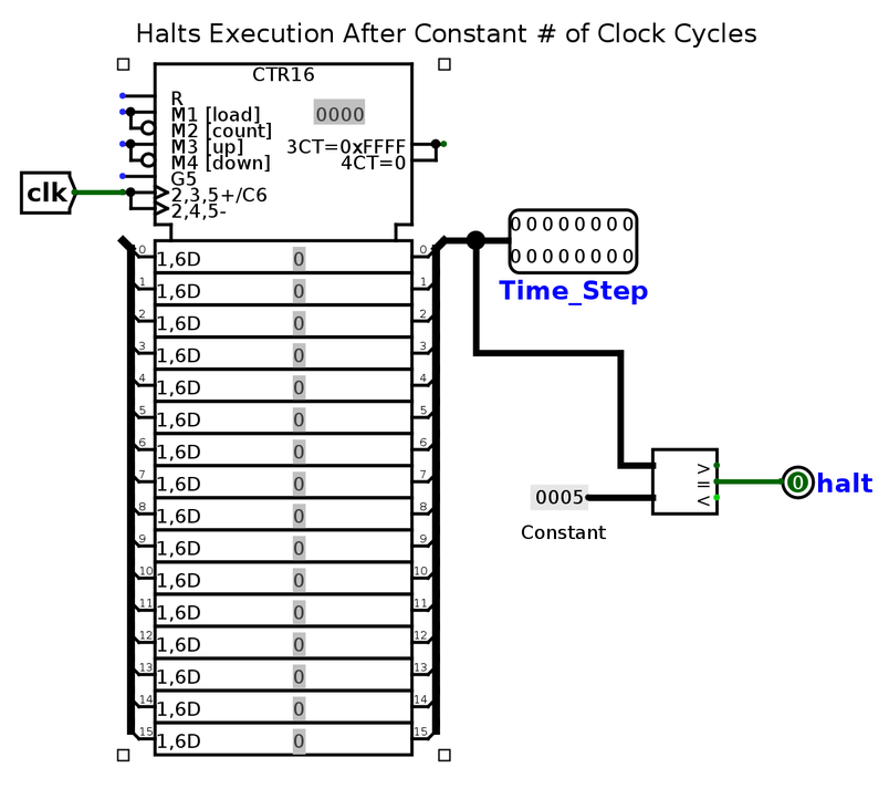
So what happens when the clock ticks? Each tick of the clock increments an input in the test file called Time_Step. The clock will continue to tick until Time_Step is equal to the halting constant for that test file (for this particular test file, the halting constant is 5). At that point, the Logisim Evolution command line will print the values in each of your outputs to stdout. Our tests will compare this output to the expected; if your output is different, you will fail the test.
ADDI Tests
We’ve included 2 tests for ADDI instruction with the starter code: one for a single-cycle CPU and one for a pipelined CPU. You can run them with the following commands:
./cpu-part1-single.sh       # For a single-cycle CPU
./cpu-part1-pipelined.sh    # For a pipelined CPU
You can see the .s RISC-V files and .hex for the test in part1-tests/addi-tests/input.
We’ve included a Python script to interpret your output: binary_to_hex.py. To use the script to see your CPU’s output, run the following commands:
$ cd part1-tests/addi-tests
$ python3 binary_to_hex.py circ_files/student_output/CPU-addi-single.out        # For a single-cycle CPU
$ python3 binary_to_hex.py circ_files/student_output/CPU-addi-pipelined.out     # For a pipelined CPU
or, to see the reference output, use this command:
$ python3 binary_to_hex.py circ_files/reference_output/CPU-addi-single.out      # For a single-cycle CPU
$ python3 binary_to_hex.py circ_files/reference_output/CPU-addi-pipelined.out   # For a pipelined CPU
Grading
Your final submission for this project will be on Gradescope. It will be available shortly. You and your project partner should have one submission; one partner should add the other to their Group on Gradescope. For Project 3-1, we’ve released all of the tests – your score on the autograder will be your final score on this part of the project. Project 3-1 will be worth 25% of your final Project 3 grade, with potential for up to 3% extra credit if you correctly implement mulh as part of your ALU.