Part B: More Instructions
In this part, you will expand your CPU to support more instructions and pipelining.
You can implement the instructions in any order you want (see the appendix for a full list of instructions and subcircuit definitions). If you'd like a bit more guidance, this spec helps you build up your CPU with small groups of instructions at a time.
Task 6: I-type Instructions
The instructions you need to implement for this task are listed below:
| Instruction | Type | Opcode | Funct3 | Funct7/Immediate | Operation |
| addi rd, rs1, imm | I | 0x13 | 0x0 | R[rd] ← R[rs1] + imm | |
| slli rd, rs1, imm | 0x1 | 0x00 | R[rd] ← R[rs1] << imm | ||
| slti rd, rs1, imm | 0x2 | R[rd] ← (R[rs1] < imm) ? 1 : 0 | |||
| xori rd, rs1, imm | 0x4 | R[rd] ← R[rs1] ^ imm | |||
| srli rd, rs1, imm | 0x5 | 0x00 | R[rd] ← R[rs1] >> imm | ||
| srai rd, rs1, imm | 0x5 | 0x20 | R[rd] ← R[rs1] >> imm | ||
| ori rd, rs1, imm | 0x6 | R[rd] ← R[rs1] | imm | |||
| andi rd, rs1, imm | 0x7 | R[rd] ← R[rs1] & imm |
Recall that you already implemented addi in Part A. These I-type instructions use the same datapath as addi, so your datapath already supports them!
Control Logic
As you add logic to support more instructions in the next few tasks, you will need to add control logic to enable the relevant datapath components depending on the instruction being executed.
The control logic should take the instruction bits and output all the control signals needed to execute that instruction. There are two main approaches to implementing this logic:
-
Suggested: Read-only memory (ROM): Hard-code a table of control signals. The relevant bits of the instruction are used to index into the table and find the control bits. See "Control Logic: Getting Started with ROM" for more information.
Pros: Fewer wires, more hard-coding (makes the control logic easier to debug).
Cons: ROM is common for CISC ISAs (like x86) but is less common for RISC ISAs (like RISC-V). Newer to this project (and may have some bugs we haven't discovered yet).
-
Alternate: Hard-wired control: Use logic gates (e.g. AND/OR/NOT gates, MUXes) to calculate the control bits from the instruction.
Pros: Used in real-world RISC-V systems, used in all past semesters.
Cons: More wires (harder to debug). Creating boolean equations with logic gates to calculate control bits generally takes longer than hardcoding bits in the ROM.
Regardless of which approach you choose, you should modify control_logic.circ in each task to implement your control logic.
Here is a summary of the control signals you should implement:
| Signal | Bit Width | Purpose |
PCSel |
1 | Selects the ALU input for all SB-type instructions where the branch is taken (according to the branch comparator output). Selects the PC+4 input for all other instructions. |
ImmSel |
1 | Selects the instruction format so the immediate generator can extract the immediate correctly. |
RegWEn |
1 | 1 if the instruction writes to a register, and 0 otherwise. |
BrUn |
1 | 1 if the branch instruction is unsigned, and 0 if the branch instruction is signed. Don't care for all other instructions. |
ASel |
1 | Selects whether to send the data in rs1 or the PC to the ALU. |
BSel |
1 | Selects whether to send the data in rs2 or the immediate to the ALU. |
ALUSel |
4 | Selects the correct operation for the ALU. |
MemRW |
1 | 1 if the instruction writes to memory, and 0 otherwise. |
WBSel |
2 | Selects whether to write the memory read from DMEM, the ALU output, or PC+4 to rd. |
Control Logic: Getting Started with ROM
-
control-logic.circalready has an empty ROM. To complete the control logic using ROM, you need to do the following:We've created a spreadsheet to help you fill in the ROM. To generate data for the ROM, you should do the following: 1. Make a copy of the spreadsheet 2. For each instruction, fill in all columns under the "Control Signals" header (RegWEn through CSRWen). Enter binary digits without the leading `0b` (Ex: type `01` instead of `0b01`). If the upper-right corner of the control signal's cell turns red, or if you see a warning when you hover over the cell, your cell contents are invalid. Common sources of errors include entering a control signal that has too many or too few bits, or entering characters other than `0` or `1` in a control logic cell.After you've filled out the spreadsheet from step 1, look for the column named "Rom Output". Copy the data in this column (not including the headers). Then, navigate to `control-logic.circ` and click on the ROM. In the properties tab on the left-hand sidebar, click on "(click to edit)" next to the "Contents" label. Click on the upper-left-most data cell (which will be a collection of 4 hex digits without a preceding `0x`) and paste your values from earlier into the ROM; you should see the ROM control bits change to the values from your spreadsheet. Click "Close Window" to exit the ROM programming view.To select a specific set of control signals for an instruction, a unique input for each instruction must be passed into the ROM. The "ROM Input" header on the spreadsheet indicates the input that must be passed into the ROM for each instruction. For example, your control logic, when passed in an `addi` instruction, needs to pass `15` (more precisely `0b1111`) into the ROM so the correct entry of control signals can be selected.To map instructions to their specific input, a Priority Encoder might be helpful! See the Example under "Tips: hard-wired control" for more information.
The `PCSel` control signal cannot be encoded in the ROM since it depends on runtime calculations performed by the processor. To complete the control logic, write hard-wired control to drive the PCSel output. -
We do not suggest modifying the inputs or outputs to the existing starter
control_logiccircuit if you are using a ROM-based implementation, since the ROM and spreadsheet cannot be easily modified to output additional control signals. If you would like to add additional control signals, we suggest using hard-wired control logic to calculate them, like you did for PCSel.
Task 6.1: Control Logic
Refer to the control logic section above for instructions.
Testing and Debugging
Before you begin, keep in mind that debugging and testing should be conducted as you are implementing your CPU. It is A LOT easier to debug one instruction type at a time versus doing them all together. If you prefer a video format, take a look at our videos on creating tests and debugging. Please note that the debugging video uses an older version of the test generation script; refer to it only for debugging and use the "creating tests" videos as a guide on how to create tests.
Here are the same instructions in written form:
We've included a script (tools/create-test.py) that uses Venus to help you generate test circuits from RISC-V assembly! The process for writing custom tests is as follows:
-
Come up with a test, and write the RISC-V assembly instructions for that test, saving them in a file ending in
.sin thetests/part-b/custom/inputs/folder. The name of this file will be the name of your test. Repeat if you have more tests.-
e.g.
tests/part-b/custom/inputs/sll-slli.sandtests/part-b/custom/inputs/beq.sNote: IMEM and DMEM are separate in Logisim, but combined in Venus. This means that if you write assembly code that tries to access memory overlapping with instructions, Venus will throw an error. Since counting exactly how many instructions your assembly code requires, and multiplying that by 4 can be annoying, we suggest you load/store using addresses greater than 0x3E8 (leaving space for 1000 bytes/250 instructions), and increase this offset if you have more instructions.
-
-
Generate the test circuits for your tests using
create-test.py:Reminder: if you want to regenerate everything, you can take advantage of Bash globs:
This should generate a couple new files to go with your assembly file:
tests/part-b/custom/: - cpu-<TEST_NAME>.circ # The new circuit for your test - inputs/<TEST_NAME>.s # The test file you wrote (unchanged) - reference-outputs/cpu-<TEST_NAME>-pipelined-ref.out # The pipelined reference output for your test - reference-outputs/cpu-<TEST_NAME>-ref.out # The single-cycle reference output for your test -
Now you can run the tests you just wrote!
Reminder: you can run all tests in a directory:
By default, the number of cycles for a test will be just enough for all instructions in the test, as well as extra cycles for the register writeback and pipelining. If you wish to override this and simulate your code for a certain number of cycles, you can use the
--cyclesflag: -
Each test will print out either:
PASSED test: <TEST_NAME> # Your student-output/<TEST_NAME>-student.out == reference-output/<TEST_NAME>-ref.out FAILED test: <TEST_NAME> Your student-output/<TEST_NAME>-student.out != reference-output/<TEST_NAME>-ref.out -
If any of your tests fail, you will need to debug it more closely in Logisim
To debug any tests or see how the circuit is working for each instruction:
- First find out where the output of your CPU implementation diverges from the staff solution. You can compare them using the diff command against the reference output and your output.
- Open the generated .circ file using Logisim. You will now see that test harness and instruction ROM. You can now use that information from your diff to step through the circuit to where you know your circuit is malfunctioning.
- Trace your wires and check outputs that are malfunctioning. Consider all possibilities:
- If regA or regB is coming out wrong, maybe it was never set correctly
- If DMEM read is coming out wrong, maybe it was never set correctly
- If ALU output is wrong, maybe the control logic is malfunctioning
- If the instruction binary is wrong, maybe branching was not implemented correctly
- etc. etc., an important part of this project is to think about picking holes in your design and solving problems.
Task 6.2: Testing and Debugging
Refer to the testing and debugging section above for instructions.
Task 7: R-type Instructions
The instructions you need to implement for this task are listed below:
| Instruction | Type | Opcode | Funct3 | Funct7/Immediate | Operation |
| add rd, rs1, rs2 | R | 0x33 | 0x0 | 0x00 | R[rd] ← R[rs1] + R[rs2] |
| mul rd, rs1, rs2 | 0x0 | 0x01 | R[rd] ← (R[rs1] * R[rs2])[31:0] | ||
| sub rd, rs1, rs2 | 0x0 | 0x20 | R[rd] ← R[rs1] - R[rs2] | ||
| sll rd, rs1, rs2 | 0x1 | 0x00 | R[rd] ← R[rs1] << R[rs2] | ||
| mulh rd, rs1, rs2 | 0x1 | 0x01 | R[rd] ← (R[rs1] * R [rs2])[63:32] | ||
| mulhu rd, rs1, rs2 | 0x3 | 0x01 | (unsigned) R[rd] ← (R[rs1] * R[rs2])[63:32] | ||
| slt rd, rs1, rs2 | 0x2 | 0x00 | R[rd] ← (R[rs1] < R[rs2]) ? 1 : 0 (signed) | ||
| xor rd, rs1, rs2 | 0x4 | 0x00 | R[rd] ← R[rs1] ^ R[rs2] | ||
| srl rd, rs1, rs2 | 0x5 | 0x00 | (unsigned) R[rd] ← R[rs1] >> R[rs2] | ||
| sra rd, rs1, rs2 | 0x5 | 0x20 | (signed) R[rd] ← R[rs1] >> R[rs2] | ||
| or rd, rs1, rs2 | 0x6 | 0x00 | R[rd] ← R[rs1] | R[rs2] | ||
| and rd, rs1, rs2 | 0x7 | 0x00 | R[rd] ← R[rs1] & R[rs2] |
Task 7.1: Datapath
Modify your datapath in cpu.circ so that it can support R-type instructions.
If you're stuck, read further for some guiding questions. As with Task 4, it may help to think about each of the five stages for executing an instruction.
Instruction Fetch: How do R-type instructions affect the program counter?
R-type instructions always increment the program counter by 4 to fetch the next instruction, just like the addi instruction from Part A. This means we don't need to modify the program counter implementation for this task.
Instruction Decode: What do we need to read from the register file?
R-type instructions have two source registers, rs1 and rs2, that we need to read from the register file. In Part A, you split the bits from the instruction corresponding to the rs1 address and passed them to the regfile. Now, you should also split the bits from the instruction corresponding to the rs2 address and pass them to the regfile.
Execute: What two data values (A and B) should an R-type instruction input to the ALU?
R-type instructions pass the register values from the regfile into the ALU. In Part A, you already passed the first register value R[rs1] into the first input of the ALU. However, for the addi instruction, the second input of the ALU is an immediate. Since you want to support both R-type instructions and the addi instruction, you should use a multiplexer to select which input will be inputted to the ALU.
The select bit of this multiplexer is BSel. You will implement the logic for determining BSel from the instruction bits in the control logic later in this task.
Memory: Do R-type instructions write to memory?
R-type instructions do not write to memory (they write to a register on the CPU, which is different from memory). This means we don't need to modify DMEM for this task.
Write back: What data is the R-type instruction writing, and where is the instruction writing this data to?
R-type instructions take the result of the computation (from the ALU output) and write the result to the register rd. In Part A, you already implemented logic to write the ALU output into a destination register.
Task 7.2: Control Logic
Refer to the control logic section above for instructions.
Task 7.3: Testing and Debugging
Refer to the testing and debugging section above for instructions.
Task 8: SB-type Instructions
The instructions you need to implement for this task are listed below:
| Instruction | Type | Opcode | Funct3 | Funct7/Immediate | Operation |
| beq rs1, rs2, offset | SB | 0x63 | 0x0 |
if(R[rs1] == R[rs2])
PC ← PC + {offset, 1b0} |
|
| bne rs1, rs2, offset | 0x1 |
if(R[rs1] != R[rs2])
PC ← PC + {offset, 1b0} |
|||
| blt rs1, rs2, offset | 0x4 |
if(R[rs1] < R[rs2] (signed))
PC ← PC + {offset, 1b0} |
|||
| bge rs1, rs2, offset | 0x5 |
if(R[rs1] >= R[rs2] (signed))
PC ← PC + {offset, 1b0} |
|||
| bltu rs1, rs2, offset | 0x6 |
if(R[rs1] < R[rs2] (unsigned))
PC ← PC + {offset, 1b0} |
|||
| bgeu rs1, rs2, offset | 0x7 |
if(R[rs1] >= R[rs2] (unsigned))
PC ← PC + {offset, 1b0} |
Task 8.1: Branch Comparator
Fill in the branch comparator subcircuit in branch-comp.circ. This subcircuit takes two inputs and outputs the result of comparing the two inputs. We will use the output later for implementing branches.
| Signal Name | Direction | Bit Width | Description |
|---|---|---|---|
| rs1 | Input | 32 | First value to compare |
| rs2 | Input | 32 | Second value to compare |
| BrUn | Input | 1 | 1 when an unsigned comparison is wanted, and 0 when a signed comparison is wanted |
| BrEq | Output | 1 | Set to 1 if the two values are equal |
| BrLt | Output | 1 | Set to 1 if the value in rs1 is less than the value in rs2 |
Task 8.2: Immediate Generator
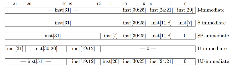
Edit the immediate generator in imm-gen.circ so that it can generate immediates for SB-type instructions in addition to immediates for I-type instructions (which you implemented in Part A).
Recall that the bits of the immediate are stored in different bits of the instruction, depending on the type of the instruction. The ImmSel signal, which you will implement in the control logic, will determine which type of immediate this subcircuit should generate.
Also, recall that all immediates are 32 bits and sign-extended.
The immediate storage formats are listed below:
Task 8.3: Datapath
Modify your datapath in cpu.circ so that it can support SB-type instructions.
If you're stuck, read further for some guiding questions. As with Task 4, it may help to think about each of the five stages for executing an instruction.
Instruction Fetch: How do SB-type instructions affect the program counter?
Recall that branching instructions add an immediate to the current value of PC. If the branch is taken, the PC changes to be the result of this addition. If the branch is not taken, or the instruction is not an SB-type instruction, then PC changes to PC+4 (just like in the previous tasks). We will implement this in the write-back stage.
Instruction Decode: What do we need to read from the register file?
SB-type instructions have two source registers, rs1 and rs2, that we need to read from the register file. In the previous task, you already implemented reading rs1 and rs2 for R-type instructions.
Execute: What two data values (A and B) should an SB-type instruction input to the ALU?
SB-type instructions use the ALU to add an immediate to PC. You will need to add a multiplexer so that the ALU can receive either PC or the value in rs1, depending on the instruction being executed. The select bit of this multiplexer is ASel. In the previous tasks, you already implemented sending an immediate to the ALU.
Memory: Do SB-type instructions write to memory?
SB-type instructions do not write to memory. This means we don't need to modify DMEM for this task.
Write back: What data is the SB-type instruction writing, and where is the instruction writing this data to?
SB-type instructions take the result of the addition (PC + immediate, from the ALU output) and might write the result to PC (depending on if the branch is taken). You should use a multiplexer to select which value will be written to PC.
The select bit of this multiplexer is PCSel. You will implement the logic for determining PCSel from the instruction bits in the control logic.
Task 8.4: Control Logic
Refer to the control logic section above for instructions.
Task 8.5: Testing and Debugging
Refer to the testing and debugging section above for instructions.
Task 9: Loading and Storing
The instructions you need to implement for this task are listed below:
| Instruction | Type | Opcode | Funct3 | Funct7/Immediate | Operation |
| lb rd, offset(rs1) | I | 0x03 | 0x0 | R[rd] ← SignExt(Mem(R[rs1] + offset, byte)) | |
| lh rd, offset(rs1) | 0x1 | R[rd] ← SignExt(Mem(R[rs1] + offset, half)) | |||
| lw rd, offset(rs1) | 0x2 | R[rd] ← Mem(R[rs1] + offset, word) | |||
| sb rs2, offset(rs1) | S | 0x23 | 0x0 | Mem(R[rs1] + offset) ← R[rs2][7:0] | |
| sh rs2, offset(rs1) | 0x1 | Mem(R[rs1] + offset) ← R[rs2][15:0] | |||
| sw rs2, offset(rs1) | 0x2 | Mem(R[rs1] + offset) ← R[rs2] |
Task 9.1: Immediate Generator
Edit the immediate generator in imm-gen.circ so that it can generate immediates for S-type instructions in addition to all the instruction types from previous tasks.
Recall that the bits of the immediate are stored in different bits of the instruction, depending on the type of the instruction. The ImmSel signal, which you will implement in the control logic, will determine which type of immediate this subcircuit should generate.
Also, recall that all immediates are 32 bits and sign-extended.
The immediate storage formats are listed below:
Conceptual Overview: Memory Unit
Since these instructions load from memory and store to memory, you will need to interact with the memory subcircuit (already implemented for you).
| Signal Name | Direction | Bit Width | Description |
|---|---|---|---|
| WriteAddr | Input | 32 | Address to read/write to in Memory |
| WriteData | Input | 32 | Value to be written to Memory |
| Write_En | Input | 4 | The write mask for instructions that write to Memory and zero otherwise |
| CLK | Input | 1 | Driven by the clock input to the CPU |
| ReadData | Output | 32 | Value of the data stored at the specified address |
Due to Logisim size limitations, the memory unit only uses the lower 16 bits of the provided address, discarding the upper 16 bits. This means that the memory can only store 2^16 bytes of data. The provided tests will always set the upper 16 bits of addresses to 0, and your tests should avoid using the upper 16 bits when interacting with memory.
The memory unit will always zero out the bottom two bits of the provided address and read 4 bytes starting at this modified address. In other words, the provided address will be rounded down to the nearest multiple of 4, and 4 bytes will be read in that range of 4 bytes.
For example, if the input address WriteAddr is 0x00001007, the bottom two bits will be zeroed out to make 0x00001004, and the output ReadData will be the 4 bytes at addresses 0x00001004, 0x00001005, 0x00001006, and 0x00001007.
The same process of zeroing out the bottom two bits applies for writing data as well, but the 4-bit Write_En input lets you select which of the 4 bytes in the WriteData input are written to the 4 bytes at the zeroed-out WriteAddr address. Each bit of this write mask enables writing to the corresponding byte of the word.
For example, if the input address WriteAddr is 0x00001007, the write mask Write_En is 0b0010, and the WriteData input is 0x11223344, then the byte 0x33 will be written to 0x00001006. If Write_En was changed to 0b0011, then the byte 0x44 would also be written to 0x00001007.
Conceptual Overview: Alignment
In this project, all memory accesses will be aligned. This means that a single load or store instruction will never cross a word boundary in memory.
All lw and sw instructions will use memory addresses that end in 0b00 (accessing 0b00, 0b01, 0b02, and 0b03 in memory).
All lh and sh instructions will use memory addresses that end in either 0b00 (accessing 0b00 and 0b01) or 0b10 (accessing 0b10 and 0b11).
You should not implement any unaligned memory accesses in this project.
Task 9.2: Datapath
Modify your datapath in cpu.circ so that it can support loads and stores.
You should provide an address input WriteAddr to DMEM. Remember that the ALU calculates this address by adding the address in rs1 and the offset immediate.
For load instructions, you should also add functionality in the write-back stage so that the data outputted by DMEM (and processed by your logic in Task 9.3) is written back to the rd register.
Task 9.3: Load
Remember that the address input WriteAddr will have its bottom two bits zeroed out. The DMEM will then output ReadData, which contains 4 bytes starting at this modified address. Implement logic in cpu.circ to extract and, if needed, sign-extend the relevant byte(s) from ReadData. Only the relevant byte(s) with appropriate sign-extending should be written back to the rd register.
For completeness, a table of scenarios you need to handle is provided below:
| Instruction | Type | Opcode | Funct3 | Bottom 2 bits of address | Value to put in rd |
| lb rd, offset(rs1) | I | 0x03 | 0x0 | 0b00 | SignExt(ReadData[7:0]) |
| 0b01 | SignExt(ReadData[15:8]) |
||||
| 0b10 | SignExt(ReadData[23:16]) |
||||
| 0b11 | SignExt(ReadData[31:24]) |
||||
| lh rd, offset(rs1) | 0x1 | 0b00 | SignExt(ReadData[15:0]) |
||
| 0b10 | SignExt(ReadData[31:16]) |
||||
| lw rd, offset(rs1) | 0x2 | 0b00 | ReadData |
Task 9.3: Store
Implement logic in cpu.circ to set up the WriteData input and Write_En write mask to correctly store the data in rs2 to memory.
For completeness, a table of scenarios you need to handle is provided below:
| Instruction | Type | Opcode | Funct3 | Bottom 2 bits of address | WriteData |
Write_En |
| sb rs2, offset(rs1) | S | 0x23 | 0x0 | 0b00 | {24'b0, R[rs2][7:0]} |
0001 |
| 0b01 | {16'b0, R[rs2][7:0], 8'b0} |
0010 |
||||
| 0b10 | {8'b0, R[rs2][7:0], 16'b0} |
0100 |
||||
| 0b11 | {R[rs2][7:0], 24'b0} |
1000 |
||||
| sh rs2, offset(rs1) | 0x1 | 0b00 | {16'b0, R[rs2][15:0]} |
0011 |
||
| 0b10 | {R[rs2][15:0], 16'b0} |
1100 |
||||
| sw rs2, offset(rs1) | 0x2 | 0b00 | R[rs2] |
1111 |
Note that for any non-store instruction (i.e. when your MemRW control signal is 0), the Write_En write mask should be set to 0000.
Task 9.4: Control Logic
Refer to the control logic section above for instructions.
Task 9.5: Testing and Debugging
Refer to the testing and debugging section above for instructions.
Task 10: All Other Instructions
The instructions you need to implement for this task are listed below:
| Instruction | Type | Opcode | Funct3 | Funct7/Immediate | Operation |
| auipc rd, offset | U | 0x17 | R[rd] ← PC + {offset, 12b0} | ||
| lui rd, offset | 0x37 | R[rd] ← {offset, 12b0} | |||
| jal rd, imm | UJ | 0x6f |
R[rd] ← PC + 4
PC ← PC + {imm, 1b0} |
||
| jalr rd, rs1, imm | I | 0x67 | 0x0 |
R[rd] ← PC + 4
PC ← R[rs1] + {imm} |
Task 10.1: Datapath
Modify your datapath in cpu.circ so that it can support these instructions. Most of these instructions are already supported by your datapath so far.
To support jalr, you should connect PC+4 to your multiplexer in the write-back stage so that PC+4 can be written back to rd.
Task 10.2: Control Logic
Refer to the control logic section above for instructions.
Task 10.3: Testing and Debugging
Refer to the testing and debugging section above for instructions.
Task 11: CSRW
The instructions you need to implement for this task are listed below:
| Instruction | Type | Opcode | Funct3 | Funct7/Immediate | Operation |
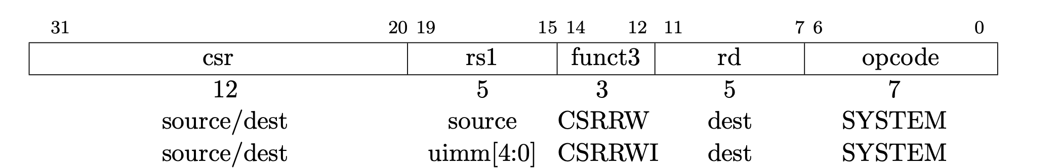
| csrw rd, csr, rs1 | I | 0x73 | 0x1 | CSR[csr] ← R[rs1] | |
| csrwi rd, csr, uimm | 0x5 | CSR[csr] ← {uimm} |
The instruction format for these instructions is shown below:
Conceptual Overview: Control Status Registers (CSRs)
Control Status Registers (CSRs) are used to hold additional information about the instructions being executed, such as debugging information or testing flags. These are unrelated to the registers and memory from the previous tasks.
To fully test your implementation, the project autograder requires one CSR (tohost = 0x51E). This means that for this project, the csr field will always be 0x51E in this project.
Also, for this project, rd will always be 0, so you don't need to worry about CSR instructions writing to a register.
Task 11.1: Immediate Generator
Edit the immediate generator in imm-gen.circ so that it can generate immediates for the csrwi instruction (in addition to all the previous immediates you've implemented).
Note that the immediate is in bits 19-15 (labeled uimm[4:0]) and should be zero-extended, not sign-extended.
Task 11.2: Datapath
Modify your datapath in cpu.circ so that it can support these instructions.
You will need to interact with the CSR subcircuit (already implemented for you).
| Signal Name | Direction | Bit Width | Description |
|---|---|---|---|
| CSR_address | Input | 12 | Input CSR register address |
| CSR_din | Input | 32 | Value to write into specified CSR register |
| CSR_WEn | Input | 1 | Write enable (from control logic) |
| clk | Input | 1 | Clock input |
| tohost | Output | 32 | Output of the tohost register |
You should connect CSR_address to the 12-bit csr field in the instruction.
For csrw instructions, CSR_din should be the data in rs1. For csrwi instructions, CSR_din should be the immediate from the immediate generator.
Task 11.3: Control Logic
Refer to the control logic section above for instructions.
Note that there are two additional control signals for the CSR instructions:
| Signal | Bit Width | Purpose |
CSRSel |
1 | Selects whether the instruction is csrw or csrwi. Don't care for all other instructions. |
CSRWen |
1 | Selects whether the instruction is a CSR instruction. 1 for csrw and csrwi, 0 otherwise. |
Task 12: Pipelining
In this task, you will implement a 2-stage pipeline in your CPU:
- Instruction Fetch: An instruction is fetched from the instruction memory.
- Execute: The instruction is decoded, executed, and committed (written back). This is a combination of the remaining four stages of a classic five-stage RISC-V pipeline (ID, EX, MEM and WB).
Some things to consider:
- Will the IF and EX stages have the same or different
PCvalues? - Do you need to store the
PCbetween the pipelining stages? - What hazards are present in this two-stage pipeline?
Note: During the first cycle, the instruction register sitting between the pipeline stages won't contain an instruction loaded from memory. What should the second stage do? Luckily, Logisim automatically sets registers to zero on reset, so the instruction pipeline register will automatically start with a nop! If you wish, you can depend on this behavior of Logisim.
Since your CPU will support branch and jump instructions, you'll need to handle control hazards that occur when branching.
-
The instruction immediately after a branch or jump should not be executed if a branch is taken. This makes your task a bit more complex. By the time you have figured out that a branch or jump is in the execute stage, you have already accessed the instruction memory and pulled out (possibly) the wrong instruction. Therefore, you will need to flush the instruction that is being fetched (next instruction) if the instruction under execution (current instruction) is a taken branch or jump.
-
Instruction flushing for this project must be accomplished by MUXing a
nopinto the instruction stream and sending thenopinto the Execute stage instead of using the fetched instruction. You can useaddi x0, x0, 0(0x00000013), for this purpose; othernopinstructions will work too. You should flush only if a branch is taken (do not flush if it is not taken). You should always flush the next instruction when jumping. -
Note: you should not solve this issue by calculating branch offsets in the IF stage. We compare your output against a reference output that uses
nop, so a solution that doesn't usenopmay not match the reference output even if it is a conceptually correct solution.
Some more things to consider:
- To MUX a
nopinto the instruction stream, do you place it before or after the instruction register? - What address should be requested next while the EX stage executes a
nop? Is this different than normal?
Testing
We've provided some basic sanity tests for your pipelined CPU in the tests/part-b/sanity/ directory (same tests as in Task 6). You can run these with:
Note: since your CPU is pipelined at this point, you need to run the pipelined tests using the --pipelined (or -p) flag. If you run the single-cycle tests (i.e. omit the --pipelined flag) after pipelining your CPU, your CPU should now fail those tests! Think about why this happens...
Similarly, you can also run the pipelined version of your custom tests:
Note: because you're implementing a 2-stage pipelined processor and the first instruction writes on the rising edge of the second clock cycle, the effects of your instructions will have a 2 instruction delay. For example, let's look at the first instruction of tests/part-b/sanity/inputs/addi.s, addi t0, x0, -1. If you inspect the pipelined reference output (tests/part-b/sanity/reference-output/cpu-addi-pipelined-ref.out), you'll see that t0 doesn't show changes until the third cycle.
Refer to the section from Project 3A for more info on using these tests. Keep in mind that you're working with a pipelined circuit from this task onward.
Task 13: Part B README Update
Time to update your README.md! Once again, write down how you implemented your circuits and components for this part (including the various subcircuits you used), and explain the reasoning behind your design choices. In particular, we want to see:
- How you designed your control logic
- Advantages/Disadvantages of your design
- Best/Worst bug or design challenge you encountered, and your solution to it
Your additions to the README should be at least 512 characters (although something more than the bare minimum would be nice), but other than that feel free to get creative!
Submission and Grading
Submit your assignment to the Project 3B submission on Gradescope. Part B is worth 80% of your overall Project 3 grade.
- Unit Tests (35%)
- Test Coverage (10%)
- Integration (5%)
- Edge (29%)
- README (1%)