CPU - Datapath and Controls
Deadline: July 31st 11:59:59 PM
Overview
In this project you will be using Logisim to implement a 32-bit two-cycle processor based on RISC-V. Once you’ve completed this project, you’ll know essentially everything you need to build a computer from scratch with nothing but logic gates!
General steps for the project:
- Get the project files
- Do the gradescope assignment
- Following the “Getting Started: A Guide” section
- Create the rest of your single-cycle processor
- Make the processor a two-stage pipeline
- Create additional unit and integration tests for your processor
- Complete!
0) Obtaining the Files
Please accept the Github classroom assignment by clicking this link. Once you’ve created your repository, you’ll need to clone it to your instructional account and/or your local machine. You’ll also need to add the starter code remote with this command:
$ git remote add staff https://github.com/61c-teach/su19-proj3-2-starter
If we publish changes to the starter code, you may get them by running git pull staff master
All the work in this project will be done from the digital logic simulation program Logisim Evolution, which is included in the starter files.
IMPORTANT: Please use the .jar file we’ve given you, not the version of Logisim that is downloaded on the lab computers! And a note: Logisim does not save your work as you go along, and it does not automatically create a new .circ file when you open it! Save when you start, and save frequently as you work.
You can open Logisim via:
$ java -jar logisim-evolution.jar
Logisim is a Java program that requires a GUI, so doing the lab over terminal
won’t work (without window forwarding, detailed below). If you wish to work on
the lab locally, ensure you have Java installed on your local machine, and pull
the latest lab starter files to your local machine. Then, you should be open
the program as above. If you wish to run the program over the terminal, you
will need to add the -X flag to your SSH command to enable window forwarding
(for example, ssh -X cs61c-xxx@...). On Windows machines, you may need to
additionally install Xming.
Important Information: Please Read!
- You are allowed to use any of Logisim’s built-in blocks for all parts of this project.
- Save frequently and commit frequently! Try to save your code in Logisim every 5 minutes or so, and commit every time you produce a new feature, even if it is small.
- Don’t move around the given inputs and outputs in your circuit; this could lead to issues with the autograder.
- Because the files you are working on are actually XML files, they’re quite difficult to merge properly. Do not work on the project in two places and attempt to merge your changes!
We will provide you with skeleton code that includes sanity tests along with a
CPU template (cpu.circ), harness (run.circ), and the data memory module
(mem.circ). You should copy your alu.circ and regfile.circ into your
Project 3-2 repository from your Project 3-1 repository. Your edits should
only be in cpu.circ, alu.circ, and regfile.circ (do not edit mem.circ
or run.circ).
Resources
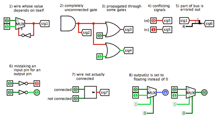
What do the different wire colors mean
Some common sources of Logisim errors, for your debugging convenience:
0.5) Gradescope Assignment
We’ve created a Gradescope assignment to get you started thinking about how to put together your CPU. We recommend finishing it before getting into the project; it’s 5% of your grade!
1) Processor
We have provided a skeleton for your processor in cpu.circ. You will be using your own implementations of the ALU and RegFile as you construct your datapath. If you find any errors in either of these components, you should definitely fix them. You are responsible for constructing the entire datapath and control from scratch. Your completed processor should implement the ISA detailed below in the section Instruction Set Architecture (ISA) using a two-stage pipeline, with IF in the first stage and ID, EX, MEM, and WB in the second stage. To start, however, we recommend you create a single-stage processor with no pipelining. Then once that is working you can modify it to become a two-stage pipeline.
Your processor will get its program from the processor harness run.circ. Your processor will output the address of an instruction, and accept the instruction at that address as an input. Inspect run.circ to see exactly what’s going on. (This same harness will be used to test your final submission, so make sure your CPU fits in the harness before submitting your work!) Your processor has 2 inputs that come from the harness:
| Input Name | Bit Width | Description |
|---|---|---|
| INSTRUCTION | 32 | Driven with the instruction at the instruction memory address identified by the FETCH_ADDRESS (see below). |
| CLOCK | 1 | The input for the clock. As with the register file, this can be sent into subcircuits (e.g. the CLK input for your register file) or attached directly to the clock inputs of memory units in Logisim, but should not otherwise be gated (i.e., do not invert it, do not AND it with anything, etc.). |
Your processor must provide the following outputs to the harness:
| Output Name | Bit Width | Description |
|---|---|---|
| ra | 32 | Driven with the contents of ra. FOR TESTING |
| sp | 32 | Driven with the contents of sp. FOR TESTING |
| t0 | 32 | Driven with the contents of t0. FOR TESTING |
| t1 | 32 | Driven with the contents of t1. FOR TESTING |
| t2 | 32 | Driven with the contents of t2. FOR TESTING |
| s0 | 32 | Driven with the contents of s0. FOR TESTING |
| s1 | 32 | Driven with the contents of s1. FOR TESTING |
| a0 | 32 | Driven with the contents of a0. FOR TESTING |
| fetch_addr | 32 | This output is used to select which instruction is presented to the processor on the INSTRUCTION input. |
Just like with the ALU and RegFile, be careful NOT to move the input or output pins!
1.5) Memory
The memory unit is already fully implemented for you! Here’s a quick summary of its inputs and outputs:
| Signal Name | Direction | Bit Width | Description |
|---|---|---|---|
| WriteAddr | Input | 32 | Address to read/write to in Memory |
| WriteData | Input | 32 | Value to be written to Memory |
| MemRW | Input | 1 | Equal to one on any instructions that write to Memory and zero otherwise |
| CLK | Input | 1 | Driven by the clock input to the CPU |
| ReadData | Output | 32 | Value of the data stored at the specified address |
Note that the address you give to memory is a byte address, but memory returns
an entire word of memory. The memory unit ignores the bottommost two bits of
the address you provide it and returns 4 bytes of data that are aligned to
addresses that are multiples of four.
A note about the lw, lh, and sw. We’ll only be implementing aligned
memory accesses in this project. This means that lw and sw will only
operate on addresses that are multiples of 4, and lh will only operate on
addresses that are multiples of 2.
2) The Instruction Set Architecture
Your CPU will support the instructions listed below. Most of the instructions should behave the same as the RISC-V you learned in class. Notice that this is not all of the instructions on the green card! These are the only instructions you will be tested on implementing, but you will not be punished for implementing other instructions (the autograder will cover ONLY the instructions below). If anything surprises you, it is likely that we made a mistake. Please make a Piazza post about it.
There is an additional instruction added to the list of R-type instructions. This is not a RISC-V instruction, but rather a new instruction created for this class, “vector add halfword”:
vaddh rd, rs1, rs2
vaddh performs two separate 16-bit additions, once on the bottom half of the
registers and once once on the top half of the registers, with the two results
concatenated and placed in the output register.
R[rd](15:0)  <-- R[rs1](15:0)  + R[rs2](15:0)
R[rd](31:16) <-- R[rs1](31:16) + R[rs2](31:16)
For example, if rs1 = 0x00010003 and rs2 = 0x00050002, the resulting value
of rd should be 0x00060005. Any carry from the addition of the lower values
should not affect the upper values. If rs1 = 0x0001FFFF and rs2 =
0x00010005 the result stored in rd should be 0x00020004.
Note: after Project 3.1 has been successfully submitted to Gradescope, you are welcome to make modifications to your ALU to rearrange instructions or add additional capabilities as you see fit, and you will need to modify your ALU to handle the new instruction.
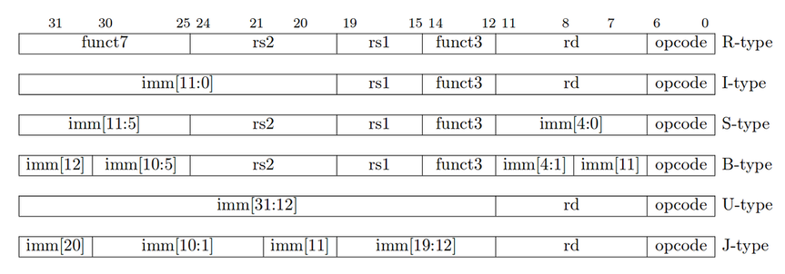
Instruction Formats
The Instructions
| Instruction | Type | Opcode | Funct3 | Funct7/Immediate | Operation |
| add rd, rs1, rs2 | R | 0x33 | 0x0 | 0x00 | R[rd] ← R[rs1] + R[rs2] |
| mul rd, rs1, rs2 | 0x0 | 0x01 | R[rd] ← (R[rs1] * R[rs2])[31:0] | ||
| vaddh rd, rs1, rs2 | 0x0 | 0x0F |
R[rd](15:0) ← R[rs1](15:0) + R[rs2](15:0)
R[rd](31:16) ← R[rs1](31:16) + R[rs2](31:16) |
||
| sub rd, rs1, rs2 | 0x0 | 0x20 | R[rd] ← R[rs1] - R[rs2] | ||
| sll rd, rs1, rs2 | 0x1 | 0x00 | R[rd] ← R[rs1] << R[rs2] | ||
| mulh rd, rs1, rs2 | 0x1 | 0x01 | R[rd] ← (R[rs1] * R [rs2])[63:32] | ||
| mulhu rd, rs1, rs2 | 0x3 | 0x01 | (unsigned) R[rd] ← (R[rs1] * R[rs2])[63:32] | ||
| slt rd, rs1, rs2 | 0x2 | 0x00 | R[rd] ← (R[rs1] < R[rs2]) ? 1 : 0 (signed) | ||
| xor rd, rs1, rs2 | 0x4 | 0x00 | R[rd] ← R[rs1] ^ R[rs2] | ||
| divu rd, rs1, rs2 | 0x5 | 0x01 | (unsigned) R[rd] ← R[rs1] / R[rs2] | ||
| srl rd, rs1, rs2 | 0x5 | 0x00 | R[rd] ← R[rs1] >> R[rs2] | ||
| or rd, rs1, rs2 | 0x6 | 0x00 | R[rd] ← R[rs1] | R[rs2] | ||
| remu rd, rs1, rs2 | 0x7 | 0x01 | (unsigned) R[rd] ← R[rs1] % R[rs2] | ||
| and rd, rs1, rs2 | 0x7 | 0x00 | R[rd] ← R[rs1] & R[rs2] | ||
| lb rd, offset(rs1) | I | 0x03 | 0x0 | R[rd] ← SignExt(Mem(R[rs1] + offset, byte)) | |
| lh rd, offset(rs1) | 0x1 | R[rd] ← SignExt(Mem(R[rs1] + offset, half)) | |||
| lw rd, offset(rs1) | 0x2 | R[rd] ← Mem(R[rs1] + offset, word) | |||
| addi rd, rs1, imm | 0x13 | 0x0 | R[rd] ← R[rs1] + imm | ||
| slli rd, rs1, imm | 0x1 | 0x00 | R[rd] ← R[rs1] << imm | ||
| slti rd, rs1, imm | 0x2 | R[rd] ← (R[rs1] < imm) ? 1 : 0 | |||
| xori rd, rs1, imm | 0x4 | R[rd] ← R[rs1] ^ imm | |||
| srli rd, rs1, imm | 0x5 | 0x00 | R[rd] ← R[rs1] >> imm | ||
| srai rd, rs1, imm | 0x5 | 0x20 | R[rd] ← R[rs1] >> imm | ||
| ori rd, rs1, imm | 0x6 | R[rd] ← R[rs1] | imm | |||
| andi rd, rs1, imm | 0x7 | R[rd] ← R[rs1] & imm | |||
| sw rs2, offset(rs1) | S | 0x23 | 0x2 | Mem(R[rs1] + offset) ← R[rs2] | |
| beq rs1, rs2, offset | SB | 0x63 | 0x0 |
if(R[rs1] == R[rs2])
PC ← PC + {offset, 1b0} |
|
| blt rs1, rs2, offset | 0x4 |
if(R[rs1] less than R[rs2] (signed))
PC ← PC + {offset, 1b0} |
|||
| bltu rs1, rs2, offset | 0x6 |
if(R[rs1] less than R[rs2] (unsigned))
PC ← PC + {offset, 1b0} |
|||
| bne rs1, rs2, offset | 0x1 |
if(R[rs1] != R[rs2])
PC ← PC + {offset, 1b0} |
|||
| lui rd, offset | U | 0x37 | R[rd] ← {offset, 12b0} | ||
| jal rd, imm | UJ | 0x6f |
R[rd] ← PC + 4
PC ← PC + {imm, 1b0} |
||
| jalr rd, rs1, imm | I | 0x67 | 0x0 |
R[rd] ← PC + 4
PC ← R[rs1] + {imm} |
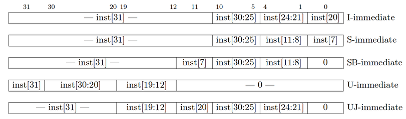
For I, S, B, U, and J type instructions, you will have to extract the appropriate immediate from the instruction. You may want to create an Immediate Generator subcircuit to do this. Remember that in RISC-V, all immediates that leave the immediate generator are 32-bits and sign-extended! You may find the following diagram helpful for thinking about how to create the appropriate immediate for each type:
3) Controls
You can probably guess that control signals will play a very large part in this project. Figuring out all of the control signals may seem intimidating. We suggest taking a look at the lecture slides to get started, and to remember that there is not a definitive set of control signals–walk through the datapath with different types of instructions, and when you see a mux or other component think about what selector/enable value you will need for that instruction. We suggest you create a “Control Module” subcircuit that takes in an instruction and outputs the control signals for that instruction.
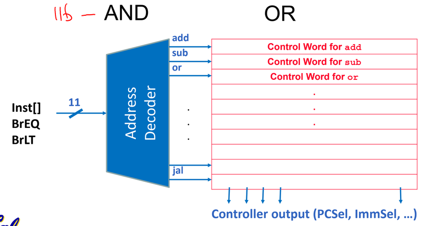
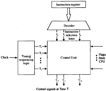
There are a two major approaches to implementing the Control so that it can translate the opcode/funct3/funct7 to the corresponding instruction and then set the control signals. One way to do it, ROM control was mentioned in lecture bonus slides. Every instruction implemented by a processor maps to an address in a ROM (read-only memory) unit. At that address in the ROM is the control word for that instruction. An address decoder takes in an instruction and outputs the address of the control word for that instruction. This approach is common in CISC architectures like Intel’s x86-64, and offers some flexibility because it can be re-programmed by changing the contents of the ROM.
The other method is hard-wired control, as discussed in lecture, which is usually the preferred approach for RISC architectures like MIPS and RISC-V. Hard-wired control uses “AND”, “OR”, and “NOT” gates (along with the various components we’ve learned can be built from these gates, like MUXes and DEMUXes) to produce the appropriate control signals. The instruction decoder takes in an instruction and outputs all of the control signals for that instruction.
The method you choose to implement your control unit is one of the major design decisions you get to make in this project.
4) Getting Started: A Guide
We know that trying to build a CPU with a blank slate might be intimidating, so we want to guide you through how to think about this project by implementing a simple I-type instruction, addi.
Recall the five stages of the CPU pipeline:
- Instruction Fetch
- Instruction Decode
- Execute
- Memory
- Write Back
This guide will help you work through each of these stages, as it pertains to the addi instruction. Each section will contain questions for you to think through and pointers to important details, but it won’t tell you exactly how to implement the instruction.
You may need to read and understand each question before going to the next one, and you can see the answers by clicking on the question. During your implementation, feel free to place things in subcircuits as you see fit.
Stage 1: Instruction Fetch
The main thing we are concerned about in this stage is: how do we get the current instruction? From lecture, we know that instructions are stored in the instruction memory, and each of these instructions can be accessed through an address.
1. Which file in the project holds your instruction memory? How does it connect to your cpu.circ file?
The instruction memory is the ROM module in `run.circ`. It provides an input into your CPU named "Instruction" and takes an output from your CPU named "fetch_addr".2. In your CPU, how would changing the address you output to fetch_addr affect the instruction input?
The instruction that `run.circ` outputs to your CPU should be the instruction at address `fetch_addr` in instruction memory.3. How do you know what the fetch_addr should be? (Hint: it is also known as PC)
`fetch_addr` is the address of the current instruction being executed, so it is saved in the PC register. For this project, it's fine for the PC to start at 0, and that is the default value for registers.4. For this project, does your PC hold an address of a byte or a word?
If you look in `run.circ`, you will see that the address coming from your CPU has the bottommost two bits truncated from it, and then goes into the memory module which holds full words (32-bits) of data. So, `fetch_addr` is a byte address, but the memory only retrieves instructions aligned to four-byte boundaries. Whether PC is a word or a byte address is up to you as the hardware designer, but keep in mind that instructions that write PC + 4 back to the RegFile are treating PC like a byte address.5. For basic programs without any jumps or branches, how will the PC change from line to line?
The PC must increment by 1 instruction in order to go to the next instruction, as the address held by the PC register represents what instruction to execute.
We have provided the PC register in the cpu.circ file. Please implement the PC’s behavior for simple programs - ignoring jumps and branches. You will have to add in the latter two in the project, but for now we are only concerned with being able to run strings of addi instructions. Where should the output of the PC register go? Remember to connect the clock!
Remember that we will in the end implement a 2-stage pipelined processor, so the IF stage is separate from the remaining stages. What circuitry separates the different stages of a pipeline? Will you need to add anything?
Stage 2: Instruction Decode
Now that we have our instruction coming from the instruction input, we have break it down in the Instruction Decode step, according to the RISC-V instruction formats you have learned.
1. What type of instruction is addi? What are the different bit fields and which bits are needed for each?
I type. The fields are: - `imm [31-20]` - `rs1 [19-15]` - `funct3 [14-12]` - `rd [11-7]` - `opcode [6-0]`2. In Logisim, what tool would you use to split out different groups of bits?
Splitter!4. Now we need to get the data from the corresponding registers, using the register file. Which instruction fields should be connected to the register file? Which inputs of the register file should it connect to?
Instruction field `rs1` will need to connect to read register 1.6. What does the Immediate Generator need to do?
For addi, the immediate generator takes in 12 bits and produces a signed 32-bit immediate. We highly suggest you create an Immediate Generator subcircuit!Stage 3: Execute
The Execute stage, also known as the ALU stage, is where the computation of most instructions is performed. This is also where we will introduce the idea of using a Control Module.
1. For the add instruction, what should be your inputs in to the ALU?
Read Data 1 and the immediate produced by the Immediate Generator.2. In the ALU, what is the purpose of ALU_Sel?
It chooses which operation the ALU should perform.3. Although it is possible for now to just put a constant as the ALUSel, why would this be infeasible as you need to implement more instructions?
With more instructions, the input to the ALU might need to change, so you would need to have some sort of circuit that changes ALUSel depending on the instruction being executed.Stage 4: Memory
The memory stage is where the memory can be written to using store instructions and read from using load instructions. Because the addi instruction does not use memory, we will not spend too much time here.
Bring in the MEM module that we provided. At this point, we cannot connect most of the inputs, as we don’t know where they should come from. However, you can still connect the clock.
Stage 5: Write back
The write back stage is where the results of the operation is saved back to the registers. Although not all instructions will write back to the register file (can you think of some which do not?), the addi instruction does.
1. Looking at the entire ISA, what are some of the instructions that will write back to a register? Where in the datapath would it get the values?
`addi` is an example that will take the output from the ALU and write it back. `lhu` will take the output from MEM and write it to a register.3. What should you use as the Select input to the MUX? What does the input depend on?
This input should be able to choose between the two MUX inputs, ALU and MEM, which means that its value depends on which instruction is executing. This suggests that the input should originate from the Control Module, as the Control Module is responsible for figuring out which instruction is executing. We'll need another control signal here, commonly called WBSel. WBSel determines which value to write back to the RegFile.4. Now that we have the inputs to the MUX sorted out, we need to wire the output. Where should the output connect to?
Because the output is the data that you want to write into the Register File, it should connect to the Write Data input on the Register File.
If you have done all of the following steps correctly, you should have a processor that works for addi instructions. You can run ./cpu-onestage-sanity.sh and see if it’s working correctly! You should pass the first test: CPU-addi. For the rest of the project, you will be implementing more instructions in much the same way–connecting outputs to inputs, adding MUXes and other Logisim components, and defining new control signals. Hopefully, this will be an easier task now that you have a basic skeleton to work off of. Good luck!
5) Pipelining
We recommend that you first implement the entire processor, and then after it is successfully working, you should pipeline it by adding the necessary registers. When you do, you will be implementing a 2-stage pipeline:
1. Instruction Fetch: An instruction is fetched from the instruction memory. (Note: while you can, please do not calculate jump address in this stage. Instead, you should try to deal with the jump control hazard.)
2. Execute: The instruction is decoded, executed, and committed (written back). This is a combination of the remaining stages of a normal five-stage RISC-V pipeline.
First, make sure you understand what hazards you will have to deal with.
The instruction immediately after a branch or jump is not executed if a branch is taken. This makes your task a bit more complex. By the time you have figured out that a branch or jump is in the execute stage, you have already accessed the instruction memory and pulled out (possibly) the wrong instruction. You will therefore need to “kill” instruction that is being fetched if the instruction under execution is a jump or a taken branch. Instruction kills for this project MUST be accomplished by MUXing a nop into the instruction stream and sending the nop into the Execute stage instead of using the fetched instruction. Notice that 0x00000013, or addi x0, x0, 0 is a nop instruction; you should only kill if a branch is taken (do not kill otherwise). Do kill on every type of jump.
Do not solve this issue by calculating branch offsets in the IF stage. Because we test your output against the reference every cycle, and the reference returns a nop, while it may be a conceptually correct solution, this will cause you to fail our tests.
Because all of the control and execution is handled in the Execute stage, your processor should be more or less indistinguishable from a single-cycle implementation, barring the one-cycle startup latency and the branch/jump delays. However, we will be enforcing the two-stage pipeline design. Some things to consider:
- Will the IF and EX stages have the same or different
PCvalues? - Do you need to store the
PCbetween the pipelining stages? - To MUX a
nopinto the instruction stream, do you place it before or after the instruction register? - What address should be requested next while the EX stage executes a
nop? Is this different than normal?
You might also notice a bootstrapping problem here: during the first cycle, the instruction register sitting between the pipeline stages won’t contain an instruction loaded from memory. How do we deal with this? It happens that Logisim automatically sets registers to zero on reset; the instruction register will then contain a nop. We will allow you to depend on this behavior of Logisim. Remember to go to Simulate --> Reset Simulation (Ctrl+R) to reset your processor.
After pipelining your processor, you should run the ./cpu-twostage-sanity.sh test instead of the single-stage version.
Testing
Understanding how the tests work
Each test is a copy of the run.circ file included with the starter code that has instructions loaded into its IMEM. When you run logisim-evolution from the command line, the clock ticks, the program counter is incremented, and the values in each of the outputs is printed to stdout.
Let’s take as an example one of the 6 sanity tests included with the starter code, CPU_addi.circ. This is a very simple test that has 3 addi instructions (addi t0, x0, 5, addi t1, t0, 7, addi s0, t0, 9), meant for a first sanity check after you go through the “Getting Started” guidelines above.
If you open onestage-tests/circ_files/CPU_addi.circ in Logisim Evolution, it’ll look like this:
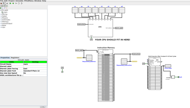
Let’s take a closer look at the various parts of the test file. At the top, you’ll see the place where your CPU is connected to the test outputs. With the skeleton file, you’ll see all xxxx’s, as you do below; when your CPU is working, this should not be the case. Your CPU takes in one input (instruction), and along with the values in each of the registers, it has one additional output: fetch_addr, or the address of the instruction to be fetched from IMEM to be executed the next clock cycle.
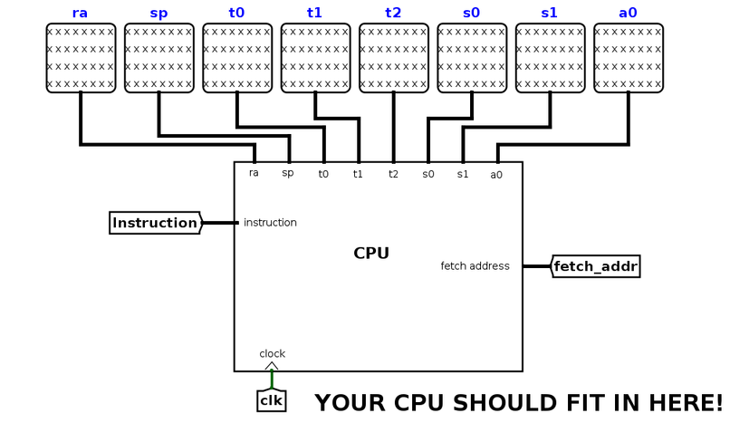
Be careful that you don’t move any of the inputs/outputs of your CPU around, or add any additional inputs/outputs. This will change the shape of the CPU subcircuit, and as a result the connections in the test files may no longer work properly.
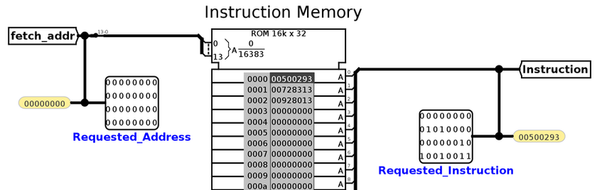
Below the CPU, you’ll see instruction memory. The hex for the 3 addi instructions (0x00500293, 0x00728313, 0x00928413) has been loaded into instruction memory. Instruction memory takes in one input (called fetch_addr) and outputs the instruction at that address. fetch_addr is a 32-bit value, but because Logisim Evolution caps the size of ROM units at 2^16B, we have to use a splitter to get only 14 bits from fetch_addr (ignoring the bottommost two bits). Notice that fetch_addr is a byte address, not a word address.
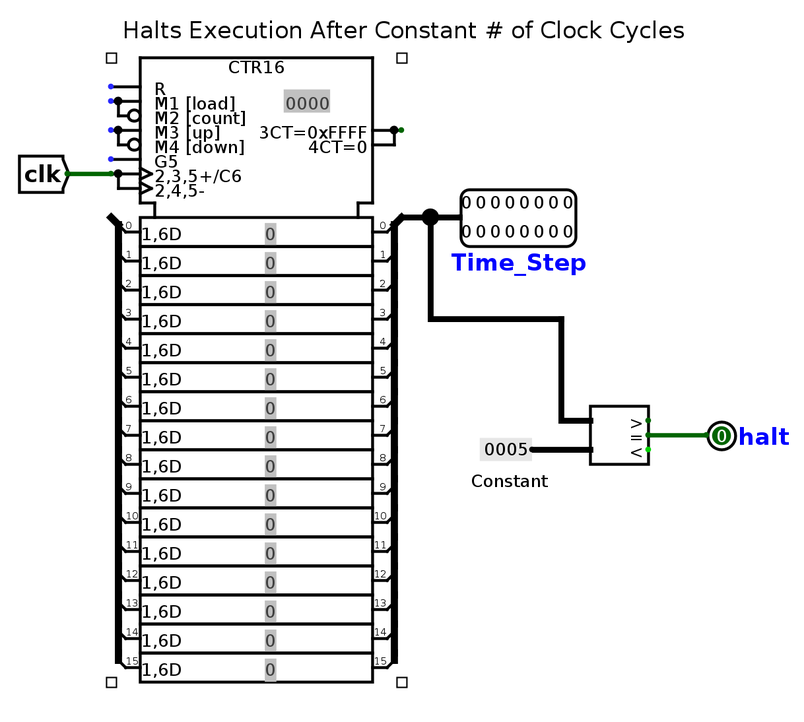
So what happens when the clock ticks? Each tick of the clock increments an input in the test file called Time_Step. The clock will continue to tick until Time_Step is equal to the halting constant for that test file (for this particular test file, the halting constant is 5). At that point, the Logisim Evolution command line will print the values in each of your outputs to stdout. Our tests will compare this output to the expected; if your output is different, you will fail the test.
Sanity Tests
We’ve included 6 sanity tests for you with the starter code. You can run them using ./cpu-onestage-sanity.sh (or with ./cpu-twostage-sanity.sh once you pipeline your processor)
Six sanity tests have been included for you with the starter code: CPU-addi.circ, CPU-add_lui_sll.circ, CPU-mem.circ, CPU-branch.circ, CPU-br_jalr.circ, and CPU-jump.circ. You can see the .s files and hex corresponding to each of these tests in the onestage-tests/input directory. Run them using the following command from your main Project 3-2 directory:
$ ./cpu-onestage-sanity.sh
Like in Project 3-1, we’ve included a Python script to make it a bit easier to interpret your test output. It’s called binary_to_hex.py. It is in the onestage-tests/circ_files directory. You can run it on the reference output for CPU-addi.circ with the following command:
$ python3 binary_to_hex.py reference_output/CPU-addi.out
or, on your CPU’s output with the following command:
$ python3 binary_to_hex.py output/CPU-addi.out
Writing your own tests
The autograder tests fall into 3 main categories: unit tests, integration tests, and edge case tests. We won’t be revealing to you what these tests are specifically, but you should be able to re-create a very close approximation of them on your own in order to test your datapath.
What is a unit test? A unit test exercises your datapath with a single instruction, to make sure that each individual instruction has been implemented and is working as expected. You should write a different unit test for every single instruction that you need to implement, and make sure that you test the spectrum of possibilities for that instruction thoroughly. For example, a unit test slt should contain cases where rs1 < rs2, rs1 > rs2, and where rs1 == rs2.
What is an integration test? After you’ve passed your unit tests, move onto tests that use multiple functions in combination. Try out various simple RISC-V programs that run a single function; your CPU should be able to handle them, if working properly. Feel free to use riscv-gcc to compile C programs to RISC-V, but be aware of the limited instruction set we’re working with (you don’t have any ecall instructions, for example).
Finally, edge cases! What edge cases should you look for? A hint from us: our 2 main classes of edge cases come from memory operations and branch/jump operations (we call them something along the lines of “mem-full” and “br-jump-edge”). Think about all the different ways these operations could go wrong.
Creating your tests
For this project, we will not be releasing all the tests. However, we have included some scripts to make test creation a little bit easier on you for two-stage processors. Included in the starter code is a file called create_test.py. It expects 1 argument: .s files containing the RISC-V code you wish to test. The script will then generate copies of run.circ with your new tests loaded in for you, along with some other files. For everything to work properly:
- Write your tests and name them whatever you would like, but be sure to save them as .s files
- Don’t move the tests anywhere, keep them (as well as
create_test.py) in the root directory of the project - Run:
$ python3 create_test.py <test 1 name here>.s <test 2 name here>.s ...
Your file hierarchy should now contain some new things:
su19-proj3-2-starter
        -- <test name here>.s  # Your test
        -- my_tests
          -- circ_files
            -- <alu, cpu, mem, regfile>.circ  # All your circuits
            -- output
            -- reference_output
            -- CPU-<test name here>.circ  # The new circuit containing your test
         -- input
            -- <test name here>.hex  # The hex dissasembly of your test
            -- <test name here>.s  # A copy of your test
Now that everything is created, to test your own tests, run:
$ ./cpu-twostage-user.sh
If you wish to delve into your the circuit running your test, you can simulate it by opening up the CPU-<test name here>.circ file. If you don’t remember how to simulate your circuit, please refer back to the Logism lab. We highly encourage you to poke your circuit while the test is running to observe how your circuit reacts to various inputs (perhaps this can give you ideas for new tests to write).
If you wish to simulate your code only for a certain number of cycles, you can do that by running the following:
$ python3 create_test.py <test name here>.s -n <number of cycles>
If you would like to decode your output, use the provided binary_to_hex.py on the appropriate .out file in the output folder shown above. Be aware that because you’re implementing a 2-stage pipelined processor and the first instruction writes on the rising edge of the second clock cycle, the effects of your instructions will have a 2 instruction delay. For example, let’s say I have written a test with one instruction:
addi t0, x0, 1
The output will actually come out to be:

Note how t0 doesn’t get changed until line 3.
NOTE: This testing harness assumes you have the 2-stage pipeline implemented. You should first concern yourself with getting the single-cycle working, then the 2-stage, then the sanity tests, and then your own tests. The sanity tests do NOT test every instruction mentioned in the spec, so make sure you are writing extra tests!
Our testing harness is using some features of Venus that are still in beta. If you have find any bugs, please let us know on Piazza. Thank you!
Grading
20% of Project 3 was Project 3-1, the RegFile and ALU. There was a potential for 3% extra credit if you implemented signed mulh properly.
The remaining 80% comes from Project 3-2. Of this 80%, 5% comes from the introductory Gradescope assignment, 25% comes from the public sanity tests, and 50% comes from the hidden unit and integration tests.
It is possible to receive the 25% for sanity tests while only creating a single-stage processor, but to receive points on the hidden tests, your processor must be a two-stage processor that is pipelined as described above. We have outlined our approach to testing in the Testing section, and if you write a thorough suite of your own tests, you should be able to pass all of the autograder tests.
Submission
Submission will be through Gradescope. The only files you should be editing are
cpu.circ, alu.circ, and regfile.circ. When you upload your code, we will
grab these files only, combine them with a default version of run.circ and
mem.circ, and run tests on them. The public sanity tests that are run on
Gradescope are identical to the cpu-onestage-sanity.sh and
cpu-twostage-sanity.sh tests.
Be sure not to make any edits to run.circ or mem.circ, or else your files
will not work in the autograder! Also be sure not to modify any of the given
inputs and outputs of cpu.circ or else the autograder will likely fail for
you.