Part A
Task 1: Arithmetic Logic Unit (ALU)
Your first task is to create an ALU that supports all the operations needed by the instructions in our ISA (which is described in further detail in the next section). Please note that we treat overflow as RISC-V does with unsigned instructions, meaning that we ignore overflow.
We have provided a skeleton of an ALU for you in alu.circ (in the cpu folder). It has three inputs:
| Input Name | Bit Width | Description |
|---|---|---|
| A | 32 | Data to use for Input A in the ALU operation |
| B | 32 | Data to use for Input B in the ALU operation |
| ALUSel | 4 | Selects which operation the ALU should perform (see the list of operations with corresponding switch values below) |
... and one output:
| Output Name | Bit Width | Description |
|---|---|---|
| Result | 32 | Result of the ALU operation |
Below is the list of ALU operations for you to implement, along with their associated ALUSel values. All of them are required. You are allowed and encouraged to use built-in Logisim components to implement the arithmetic operations.
| ALUSel Value | Instruction |
|---|---|
| 0 | add: Result = A + B |
| 1 | sll: Result = A << B |
| 2 | slt: Result = (A < B (signed)) ? 1 : 0 |
| 3 | Unused |
| 4 | xor: Result = A ^ B |
| 5 | srl: Result = (unsigned) A >> B |
| 6 | or: Result = A | B |
| 7 | and: Result = A & B |
| 8 | mul: Result = (signed) (A * B)[31:0] |
| 9 | mulh: Result = (signed) (A * B)[63:32] |
| 10 | Unused |
| 11 | mulhu: Result = (A * B)[63:32] |
| 12 | sub: Result = A - B |
| 13 | sra: Result = (signed) A >> B |
| 14 | Unused |
| 15 | bsel: Result = B |
The ALU tests for Part A only use ALUSel values for defined instructions, so your design doesn't need to worry about the unused values.
You can make any modifications to alu.circ you want, but the behavior must match the specification above. If you create additional subcircuits for your ALU, they must also be in alu.circ (you may not make new .circ files). Additionally, your ALU must be able to fit in the provided harness alu-harness.circ. This means that you should take care not to edit the provided input/output pins or add new ones. To verify that changes you made didn’t break anything, you can open alu-harness.circ and ensure there are no errors and that the circuit functions well.
Tips
addis already made for you; feel free to use a similar structure when implementing your other operations.- If you want to know more details about each component, go to
Help -> Library Referencefor more information on the component and its inputs and outputs. - You might find bit splitters or extenders useful when implementing shift operations.
- Use tunnels! They will make your wiring cleaner and easier to follow, and will reduce your chances of encountering crossed wires or unexpected errors.
- Ensure you name your tunnels correctly. The labels are case sensitive!
- The result of multiplying 2 32-bit numbers can be up to 64 bits of information, but we're limited to 32-bit data lines, so
mulhandmulhuare used to get the upper 32 bits of the product. The Library Reference might help with these operations. - You can hover your cursor over an input/output on a component to get slightly more information about that input/output. For example, the
Multipliercomponent has aCarry Outoutput, with the description: "the upper bits of the product". This might be particularly useful for certain multiply operations. - A multiplexer (MUX) might be useful when deciding between operation outputs. In other words, consider simply processing the input for all operations, and then outputting the one of your choice.
- The comparator component might be useful for implementing instructions that involve comparing inputs. Reference the table above to see if it's required in the ALU.
Info: Testing
Here's a companion video that goes with this section.
We've provided some tests for each task, located in subdirectories under tests/. For example, the ALU tests are in tests/part-a/alu/. When these tests are run, the outputs from your circuits are saved in a tests/part-a/alu/student-output/ subdirectory.
For example, to run the ALU tests:
$ python3 test.py tests/part-a/alu/
You can also specify a single test circuit, or a grandparent/great-grandparent directory:
$ python3 test.py tests/part-a/alu/alu-add.circ
$ python3 test.py tests/part-a/
$ python3 test.py tests/
After the tests finish running, your ALU circuit's outputs will be saved under tests/part-a/alu/student-output/ with a -student.out suffix (e.g. alu-add-student.out). The corresponding reference outputs can be found at tests/part-a/alu/reference-output/ with a -ref.out suffix (e.g. alu-add-ref.out).
We've also provided format-output.py, which accepts a path to an output file and displays the output in a more readable format (left-aligned hexadecimal numbers). For example, to get the reference output of the alu-add sanity test in readable format, you would do:
$ python3 tools/format-output.py tests/part-a/alu/reference-output/alu-add-ref.out
If you want to see the difference between your output and the reference solution, you can put the readable outputs into temporary files and diff them. For example, for the alu-add test, you would do:
$ python3 tools/format-output.py tests/part-a/alu/reference-output/alu-add-ref.out > reference.out
$ python3 tools/format-output.py tests/part-a/alu/student-output/alu-add-student.out > student.out
$ diff reference.out student.out
Note: If the lines are wrapping, try resizing your terminal window (or try a slightly smaller font). Or see the following note.
Experimental Note
Here's a companion video that goes with this note.
Each output file is technically a valid CSV file, so you can also import the output in a spreadsheet app if you really want to crunch the numbers (or you really hate tables in terminal). If the app requires a .csv extension, you can use
cp tests/part-a/alu/student-output/alu-add-student.out student.csv
and import the resulting .csv file.
Inspecting Tests
Here's a companion video that goes with this section.
Similar to how you can step through your C code in GDB, you can also step through the test circuits in Logisim! For this example we'll be using the alu-add test.
Open tests/part-a/alu/alu-add.circ in Logisim. Among other things, one ROM (read-only memory) each feeds into the Input_A, Input_B, and ALUSel tunnels. These tunnels then feed into your ALU near the upper right. The ROMs contain corresponding values for the test being considered. Every clock cycle, the adder on the top left increments by one, which advances each ROM by one entry, thus feeding the next set of inputs to your ALU. If you tick the circuit a couple times (File -> Tick Full Cycle or the corresponding keyboard shortcut), you can see the test circuit advance through each set of inputs and your ALU's corresponding outputs. If you want to start over, use Simulate -> Reset Simulation (Command/Control + R).
Now, let's see what your ALU is actually doing with the inputs. Right-click your ALU, and select View alu. Your ALU circuit will appear, with the input values for the current test cycle already on the ALU input pins. With this, you can see exactly what your ALU is doing in every line from the output files! The Poke Tool will be very useful here.
Note: Edits to the test circuit, including the ALU we just inspected, will not be saved. Avoid making edits in the test circuit, as they may be lost!
Task 2: Register File (RegFile)
As you learned in class, RISC-V architecture has 32 registers. For this project, we will implement all of them. To aid in debugging and testing, we have written the RegFile to expose the 8 registers specified below. These registers are exposed using output pins. You must ensure that you connect these output pins to their corresponding registers.
- Your RegFile should be able to write to or read from these registers specified in a given RISC-V instruction without affecting any other registers.
- There is one notable exception: your RegFile should NOT write to x0, even if an instruction tries. Remember that the zero register should ALWAYS have the value 0x0.
- Gating the clock signal means passing it through combinational logic before further use. You should NOT gate the clock at any point in your RegFile. The clock signal should ALWAYS connect directly to the clock input of the registers without passing through ANY combinational logic.
The exposed registers and their corresponding numbers are listed below.
| Register Number | Register Name |
|---|---|
| x1 | ra |
| x2 | sp |
| x5 | t0 |
| x6 | t1 |
| x7 | t2 |
| x8 | s0 |
| x9 | s1 |
| x10 | a0 |
You are provided with the skeleton of a register file in regfile.circ. The register file circuit has six inputs:
| Input Name | Bit Width | Description |
|---|---|---|
| Clock | 1 | Input providing the clock. This signal can be sent into subcircuits or attached directly to the clock inputs of memory units in Logisim, but should not otherwise be gated (i.e., do not invert it, do not AND it with anything, etc.). |
| RegWEn | 1 | Determines whether data is written to the register file on the next rising edge of the clock. |
| rs1 (Source Register 1) | 5 | Determines which register's value is sent to the Read_Data_1 output, see below. |
| rs2 (Source Register 2) | 5 | Determines which register's value is sent to the Read_Data_2 output, see below. |
| rd (Destination Register) | 5 | Determines which register to write the value of Write Data to on the next rising edge of the clock, assuming that RegWEn is a 1. |
| wb (Write Data) | 32 | Determines what data to write to the register identified by the Destination Register input on the next rising edge of the clock, assuming that RegWEn is 1. |
The register file also has the following outputs:
| Output Name | Bit Width | Description |
|---|---|---|
| Read_Data_1 | 32 | Driven with the value of the register identified by the Source Register 1 input. |
| Read_Data_2 | 32 | Driven with the value of the register identified by the Source Register 2 input. |
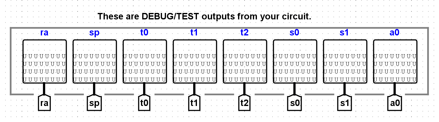
ra Value | 32 | Always driven with the value of ra (This is a DEBUG/TEST output.) |
sp Value | 32 | Always driven with the value of sp (This is a DEBUG/TEST output.) |
t0 Value | 32 | Always driven with the value of t0 (This is a DEBUG/TEST output.) |
t1 Value | 32 | Always driven with the value of t1 (This is a DEBUG/TEST output.) |
t2 Value | 32 | Always driven with the value of t2 (This is a DEBUG/TEST output.) |
s0 Value | 32 | Always driven with the value of s0 (This is a DEBUG/TEST output.) |
s1 Value | 32 | Always driven with the value of s1 (This is a DEBUG/TEST output.) |
a0 Value | 32 | Always driven with the value of a0 (This is a DEBUG/TEST output.) |
The test outputs at the top of your regfile circuit are present for testing and debugging purposes. If you were implementing a real register file, you would omit those outputs. In our case, be sure they are included correctly -- if they are not, you will not pass tests.
You can make any modifications to regfile.circ you want, but the behavior must match the specification above. If you create additional subcircuits to use in your RegFile, they must also be in regfile.circ (you may not make new .circ files). Additionally, your RegFile must be able to fit in the provided harness regfile-harness.circ. This means that you should take care not to edit the provided input/output pins or add new ones. To verify that changes you made didn’t break anything, you can open regfile-harness.circ and ensure there are no errors and that the circuit functions well.
Tips
- Take advantage of copy-paste! It might be a good idea to make one register completely and use it as a template for the others to avoid repetitive work.
- You can duplicate a selected component or group of components in Logisim using
Ctrl/Cmd + D. - MUXes will be helpful. DeMUXes may also be helpful.
- We recommend not using the
Enableinput on your MUXes. In fact, you can turn that attribute off (Include Enable?). We also recommend that you disable theThree-state?attribute (if the plexer has it). - Open up the Library Reference page for the
Registercomponent, and check out all the input/output pins. TheEnablepin may come in handy. - Think about what happens in the register file after a single instruction is executed. Which values change? Which values stay the same? Registers are clock-triggered -- what does that mean?
- What should happen if we try to write to
x0?
RegFile Testing
We've provided the autograder RegFile tests in the tests/part-a/regfile/ directory. You can run these with:
$ python3 test.py tests/part-a/regfile/
Refer to the Info: Testing section for more info on test outputs.
Task 3: The addi Instruction
As your final task for Part A, you're going to implement a CPU that's capable of executing one instruction: addi!
Note: We'll be implementing other instructions in Part B. You're welcome to implement other instructions at this time, but you'll only be graded on whether or not addi executes correctly for Part A, so make sure that addi works!
Info: Immediate Generator
The Immediate Generator ("Imm Gen") unit (located in imm-gen.circ) provided in the skeleton is unimplemented. The addi instruction requires an immediate generator, but for now you can hard-wire it to construct the immediate for the addi instruction, without worrying about other immediate types.
To edit this subcircuit, edit the imm-gen.circ file and not the imm_gen in cpu.circ. Note that if you modify this circuit, you will need to close and re-open cpu.circ to load the changes in your CPU.
Here's a quick summary of its inputs and outputs:
| Signal Name | Direction | Bit Width | Description |
|---|---|---|---|
| inst | Input | 32 | The instruction being executed |
| ImmSel | Input | 3 | Value determining how to reconstruct the immediate |
| imm | Output | 32 | Value of the immediate in the instruction |
Info: Processor
We have provided a skeleton for your processor in cpu.circ. You will be using your own implementations of the ALU and RegFile as you construct your datapath. You are responsible for constructing the entire datapath from scratch. For Part A, your completed processor should support executing the addi instruction in a single cycle (i.e. no pipelining). In Part B, we'll modify your CPU to use a 2-stage pipeline, with IF in the first stage and ID, EX, MEM, and WB in the second stage.
Your processor will sit in a processor harness cpu-harness.circ that contains the Memory unit. That processor harness then sits in a testing harness run.circ that provides the instructions to the processor. Your processor will output the address of an instruction, and accept the instruction at that address as an input. It will also output the data memory address, data memory write enable, and accept the data at that address as an input. Essentially, your processor will output instruction and data memory addresses, and the harnesses will reply with the data at those addresses.
We recommend that you take some time to inspect cpu-harness.circ and run.circ to see exactly what's going on. cpu-harness.circ will be used in the tests provided to you, so make sure your CPU fits in the harness before testing and submitting your work! Your processor has 3 inputs that come from the processor harness:
| Input Name | Bit Width | Description |
|---|---|---|
| READ_DATA | 32 | Driven with the data at the data memory address identified by the WRITE_ADDRESS (see below). |
| INSTRUCTION | 32 | Driven with the instruction at the instruction memory address identified by the PROGRAM_COUNTER (see below). |
| CLOCK | 1 | The input for the clock. As with the register file, this can be sent into subcircuits (e.g. the CLK input for your register file) or attached directly to the clock inputs of memory units in Logisim, but should not otherwise be gated (i.e., do not invert it, do not AND it with anything, etc.). |
Your processor must provide the following outputs to the processor harness:
| Output Name | Bit Width | Description |
|---|---|---|
| ra | 32 | Driven with the contents of ra (FOR TESTING) |
| sp | 32 | Driven with the contents of sp (FOR TESTING) |
| t0 | 32 | Driven with the contents of t0 (FOR TESTING) |
| t1 | 32 | Driven with the contents of t1 (FOR TESTING) |
| t2 | 32 | Driven with the contents of t2 (FOR TESTING) |
| s0 | 32 | Driven with the contents of s0 (FOR TESTING) |
| s1 | 32 | Driven with the contents of s1 (FOR TESTING) |
| a0 | 32 | Driven with the contents of a0 (FOR TESTING) |
| tohost | 32 | Driven with the contents of CSR 0x51E (FOR TESTING, for Part A leave it as-is) |
| WRITE_ADDRESS | 32 | This output is used to select which address to read/write data from in data memory. |
| WRITE_DATA | 32 | This output is used to provide write data to data memory. |
| WRITE_ENABLE | 4 | This output is used to provide the write enable mask to data memory. |
| PROGRAM_COUNTER | 32 | This output is used to select which instruction is presented to the processor on the INSTRUCTION input. |
Just like with the ALU and RegFile, make sure that you do not edit the input/output pins or add new ones!
Info: Control Logic
The Control Logic unit (control-logic.circ) provided in the skeleton is unimplemented. Designing the control logic unit will probably be your biggest challenge in Part B. For Part A, you can put a constant for each control signal, because addi is the only instruction you'll be implementing. As you implement addi, think about where you'll need to make additions in order to support other instructions.
To edit this subcircuit, edit the control-logic.circ file and NOT the control_logic in cpu.circ. Note that if you modify this circuit, you will need to close and re-open cpu.circ to load the changes in your CPU.
You are welcome to add more input/output pins to the starter control logic as your design demands. You may also use as many or as few of the supplied ports as needed. However, please do not edit any of the existing pins during this process.
Info: Memory
The addi instruction does NOT use Data Memory, so for Part A you can ignore the DMEM and leave its I/O pins undriven.
Info: Branch Comparator
The addi instruction does NOT use the Branch Comparator unit, so you don't have to worry about it for Part A.
Single Stage CPU: A Guide
We know that trying to build a CPU from a blank slate might be intimidating, so here's a guide that might help.
Recall the five stages of the CPU pipeline:
- Instruction Fetch (IF)
- Instruction Decode (ID)
- Execute (EX)
- Memory (MEM)
- Write Back (WB)
This guide will help you work through each of these stages for the addi instruction. Each section will contain questions for you to think through and pointers to important details, but it won't tell you exactly how to implement the instruction.
You may need to read and understand each question before going to the next one, and you can see the answers by clicking on the question. As you implement your CPU, feel free to place things in subcircuits as you see fit.
Stage 1: Instruction Fetch
The main thing we are concerned about in this stage is: how do we get the current instruction? From lecture, we know that instructions are stored in the instruction memory, and each of these instructions can be accessed through an address.
1. Which file in the project holds your instruction memory? How does it connect to your cpu.circ file?
The instruction memory is the ROM module in run.circ. It provides an input into your CPU named INSTRUCTION and takes an output from your CPU, called PROGRAM_COUNTER.
2. In your CPU, how would changing the address you output as PROGRAM_COUNTER affect the instruction input?
The instruction that run.circ outputs to your CPU should be the instruction at address PROGRAM_COUNTER in instruction memory.
3. How do you know what PROGRAM_COUNTER should be?
PROGRAM_COUNTER is the address of the current instruction being executed, so it is saved in the PC register. For this project, your PC will start at 0, as that is the default value for a register.
4. For basic programs without any jumps or branches, how will the PC change from line to line?
The PC must increment by 1 instruction in order to go to the next instruction, as the address held by the PC register represents what instruction to execute. Assuming no branch or jump, this means that your PC will typically increase by 4 (bytes) line to line.
In cpu.circ, we have provided a simple PC register implementation - ignoring jumps and branches. You will implement branches and jumps in Part B of the project, but for now we are only concerned with being able to run addi instructions.
Stage 2: Instruction Decode
Now that we have our instruction coming from the instruction input, we break it down in the Instruction Decode step according to the RISC-V instruction formats you have learned.
1. What type of instruction is addi? What are the different bit fields and which bits are needed for each?
I type. The fields are:
imm [31-20]rs1 [19-15]funct3 [14-12]rd [11-7]opcode [6-0]
2. In Logisim, what tool would you use to split out different groups of bits?
The Splitter!
- Implement the instruction field decode stage using the instruction input. You should use tunnels to label and group the bits.
4. Now we need to provide the appropriate inputs to the register file. Which instruction fields should connect to the register file? Which inputs of the register file should they connect to?
Instruction field rs1 should connect to the read register 1 pin.
Instruction field rd should connect to the write register pin.
Remember to connect the clock to the register file!
Since addi is an I type instruction, we do not need to worry about the read register 2 pin.
5. What does the Immediate Generator need to do?
For addi, the immediate generator takes in 12 bits from the instruction and produces a signed 32-bit immediate. You will need to implement this logic in the Immediate Generator subcircuit!
Stage 3: Execute
The Execute stage is where the computation of most instructions is performed. This is also where we will introduce the idea of using a Control Logic unit.
1. For the add instruction, what should be your inputs to the ALU?
Read Data 1 (rs1) and the immediate produced by the Immediate Generator.
2. In the ALU, what is the purpose of ALUSel?
It determines which operation the ALU will perform.
3. Although it is possible for now to just put a constant as the ALUSel, why would this be infeasible as you implement more instructions?
With more instructions, the input to the ALU might need to change, so you will need to have some sort of circuit that changes ALUSel depending on the instruction being executed.
- Bring in your ALU and connect the ALU inputs correctly.
Stage 4: Memory
The memory stage is where the memory can be written to using store instructions and read from using load instructions. Because the addi instruction does not use memory, we do not have to worry about it for Part A. Please ignore the DMEM and leave its I/O pins undriven.
Stage 5: Write Back
The write back stage is where the results of the operation is saved back to the registers.
1. Do addi instructions need to write back to a register?
Yes. addi takes the output of a an addition computation in the ALU and writes it back to the register file.
2. Since we are only implementing the addi instruction now, let's create the write back phase such that it is able to write ALU output to the Register File. Where should the ALU output connect to?
Because the output is the data that you want to write into the Register File, it should connect to the Write Data input on the Register File.
- There is one more input on the Register File which is important for writing data:
RegWEn. Sinceaddialways writes back to the Register File, you can hardwire this to a 1-bit constant with the value1.
Info: CPU Testing
In the Info: Testing section, we got to know the general directory structure of the test harness, and understand the commands involved in running tests and interpreting output. Now, let's look deeper into the CPU tests that you'll be working with for the remainder of the project.
Understanding CPU Tests
Here's a companion video that goes with this section.
Each CPU test is a copy of the run.circ file included with the starter code that has instructions loaded into its IMEM. When you run the test.py script, it runs Logisim in the background. The clock ticks, the program counter is incremented, and the values in each of the outputs is printed to a .out file in the student-outputs directory.
Let's take the single-cycle cpu-addi-basic sanity test as an example. It has 4 addi instructions (see tests/part-a/addi/inputs/cpu-addi-basic.s). Open tests/part-a/addi/cpu-addi-basic.circ in Logisim, and take a closer look at the various parts of the test file. At the top, you'll see the place where your CPU is connected to the test outputs. With the starter code, you'll see lots of UUUUs or XXXXs; when your CPU is working, this should not be the case. Your CPU takes in one input (INSTRUCTION), and along with the values in each of the registers, it has an additional output: PROGRAM_COUNTER, or the address of the instruction to be fetched from IMEM to be executed the next clock cycle.
As you can see, there are many specifically-positioned wires connected to specific input/output pins on your CPU. Make sure that you do not edit the provided input/output pins or add new ones, as this will change the shape of the CPU circuit, and as a result the connections in the test files may no longer work properly.
Below the CPU, you'll see instruction memory. The hex for the addi instructions has been loaded into instruction memory. Instruction memory takes in one input (called PROGRAM_COUNTER) and outputs the instruction at that address. PROGRAM_COUNTER is a 32-bit value, but because Logisim caps the size of ROM units at 2^16 bytes, we have to use a splitter to get only 14 bits from PROGRAM_COUNTER (ignoring the bottommost two bits). Notice that PROGRAM_COUNTER is a byte address, not a word address.
So what happens when the clock ticks? Each tick of the clock increments an input in the test file called Time_Step. The clock will continue to tick until Time_Step is equal to the halting constant for that test file (for this particular test file, the halting constant is 6). At that point, the test.py script will print the values in each of the outputs to the respective .out file. Our tests will compare this output to the expected; if your output is different, you will fail the test.
addi Tests
We've provided the autograder tests for addi (Task 3) in the tests/part-a/addi/ directory. You can run these with:
$ python3 test.py tests/part-a/addi/
Task 4: Part A README Update
Your last task for Part A is to fill in the README.md. Write down how you implemented your circuits and components for this part (including ALU and RegFile, since you used them for addi!), and explain the reasoning behind your design choices. There's no specific format or length requirement here, so feel free to get creative!
Submission
At this point, if you've completed tasks 1 through 4, you've finished Part A of the project!
The autograder for Part A uses the same tests as the test files provided in the starter code. In other words, there are no hidden tests for Part A.
Double-check that you have not edited your input/output pins, and that your circuits fit in the provided testing harnesses. Make sure that you did not create any additional .circ files; the autograder will only be testing the circuit files you were allowed to edit for Part A (alu.circ, branch-comp.circ, control-logic.circ, cpu.circ, imm-gen.circ, and regfile.circ). Then, submit your repo to the Project 3A assignment on Gradescope.
If you pipeline your CPU in Part B and then realize you want to resubmit to Part A, we've got you covered! For addi tests, the autograder accepts either a single-cycle or a pipelined CPU. Please note that the deadline for Part A still applies to such resubmissions.
Grading
Part A is worth 20% of the overall grade of the project. The grading breakdown for Part A is as follows:
- ALU (7%)
- RegFile (8%)
addi(5%)