Part B
Getting Started
Please pull the latest updates from the starter code using
git pull starter main
Task 5: More Instructions
In Task 3, you wired up a basic single-cycle CPU capable of executing addi instructions. Now, you'll implement support for more instructions!
Your CPU will end up with many parts -- try breaking it down into chunks, and start with the simple ones first. How you approach this task is entirely up to you, but one suggested starting order is: branch comparator and immediate generator (simpler than control logic/datapath), then I-type calculation instructions (since you've already implemented addi), then R-type calculation instructions (since there's some overlap with I-type calculation instructions), and so on.
You should work on Task 5 and Task 6 (Custom Tests) together, since incremental testing will help you catch bugs much faster. Write tests for an instruction (or group of instructions) you plan to implement, then implement the instruction(s) while using your tests as a reference. Once your tests pass, commit your changes so you can come back later if you find a regression, and move on to another instruction. If you wait until the end to write your tests, you are going to end up spending much longer debugging.
The Instruction Set Architecture (ISA)
We will be grading your CPU implementation on only the instructions listed below. You do not need to worry about unused opcodes. Your CPU must support these instructions, but feel free to implement any additional instructions you want as long as they don't affect your implementation of the required instructions.
| Instruction | Type | Opcode | Funct3 | Funct7/Immediate | Operation |
| add rd, rs1, rs2 | R | 0x33 | 0x0 | 0x00 | R[rd] ← R[rs1] + R[rs2] |
| mul rd, rs1, rs2 | 0x0 | 0x01 | R[rd] ← (R[rs1] * R[rs2])[31:0] | ||
| sub rd, rs1, rs2 | 0x0 | 0x20 | R[rd] ← R[rs1] - R[rs2] | ||
| sll rd, rs1, rs2 | 0x1 | 0x00 | R[rd] ← R[rs1] << R[rs2] | ||
| mulh rd, rs1, rs2 | 0x1 | 0x01 | R[rd] ← (R[rs1] * R [rs2])[63:32] | ||
| mulhu rd, rs1, rs2 | 0x3 | 0x01 | (unsigned) R[rd] ← (R[rs1] * R[rs2])[63:32] | ||
| slt rd, rs1, rs2 | 0x2 | 0x00 | R[rd] ← (R[rs1] < R[rs2]) ? 1 : 0 (signed) | ||
| xor rd, rs1, rs2 | 0x4 | 0x00 | R[rd] ← R[rs1] ^ R[rs2] | ||
| srl rd, rs1, rs2 | 0x5 | 0x00 | (unsigned) R[rd] ← R[rs1] >> R[rs2] | ||
| sra rd, rs1, rs2 | 0x5 | 0x20 | (signed) R[rd] ← R[rs1] >> R[rs2] | ||
| or rd, rs1, rs2 | 0x6 | 0x00 | R[rd] ← R[rs1] | R[rs2] | ||
| and rd, rs1, rs2 | 0x7 | 0x00 | R[rd] ← R[rs1] & R[rs2] | ||
| lb rd, offset(rs1) | I | 0x03 | 0x0 | R[rd] ← SignExt(Mem(R[rs1] + offset, byte)) | |
| lh rd, offset(rs1) | 0x1 | R[rd] ← SignExt(Mem(R[rs1] + offset, half)) | |||
| lw rd, offset(rs1) | 0x2 | R[rd] ← Mem(R[rs1] + offset, word) | |||
| addi rd, rs1, imm | 0x13 | 0x0 | R[rd] ← R[rs1] + imm | ||
| slli rd, rs1, imm | 0x1 | 0x00 | R[rd] ← R[rs1] << imm | ||
| slti rd, rs1, imm | 0x2 | R[rd] ← (R[rs1] < imm) ? 1 : 0 | |||
| xori rd, rs1, imm | 0x4 | R[rd] ← R[rs1] ^ imm | |||
| srli rd, rs1, imm | 0x5 | 0x00 | R[rd] ← R[rs1] >> imm | ||
| srai rd, rs1, imm | 0x5 | 0x20 | R[rd] ← R[rs1] >> imm | ||
| ori rd, rs1, imm | 0x6 | R[rd] ← R[rs1] | imm | |||
| andi rd, rs1, imm | 0x7 | R[rd] ← R[rs1] & imm | |||
| sb rs2, offset(rs1) | S | 0x23 | 0x0 | Mem(R[rs1] + offset) ← R[rs2][7:0] | |
| sh rs2, offset(rs1) | 0x1 | Mem(R[rs1] + offset) ← R[rs2][15:0] | |||
| sw rs2, offset(rs1) | 0x2 | Mem(R[rs1] + offset) ← R[rs2] | |||
| beq rs1, rs2, offset | SB | 0x63 | 0x0 |
if(R[rs1] == R[rs2])
PC ← PC + {offset, 1b0} |
|
| bne rs1, rs2, offset | 0x1 |
if(R[rs1] != R[rs2])
PC ← PC + {offset, 1b0} |
|||
| blt rs1, rs2, offset | 0x4 |
if(R[rs1] < R[rs2] (signed))
PC ← PC + {offset, 1b0} |
|||
| bge rs1, rs2, offset | 0x5 |
if(R[rs1] >= R[rs2] (signed))
PC ← PC + {offset, 1b0} |
|||
| bltu rs1, rs2, offset | 0x6 |
if(R[rs1] < R[rs2] (unsigned))
PC ← PC + {offset, 1b0} |
|||
| bgeu rs1, rs2, offset | 0x7 |
if(R[rs1] >= R[rs2] (unsigned))
PC ← PC + {offset, 1b0} |
|||
| auipc rd, offset | U | 0x17 | R[rd] ← PC + {offset, 12b0} | ||
| lui rd, offset | 0x37 | R[rd] ← {offset, 12b0} | |||
| jal rd, imm | UJ | 0x6f |
R[rd] ← PC + 4
PC ← PC + {imm, 1b0} |
||
| jalr rd, rs1, imm | I | 0x67 | 0x0 |
R[rd] ← PC + 4
PC ← R[rs1] + {imm} |
|
| csrw rd, csr, rs1 | I | 0x73 | 0x1 | CSR[csr] ← R[rs1] | |
| csrwi rd, csr, uimm | 0x5 | CSR[csr] ← {uimm} |
Info: Branch Comparator
The Branch Comparator unit (located in branch-comp.circ) compares two values and outputs control signals that will be used to make branching decisions. You will need to implement logic for this circuit.
To edit this subcircuit, edit the branch-comp.circ file and not the branch_comp in cpu.circ. Note that if you modify this circuit, you will need to close and re-open cpu.circ to load the changes in your CPU.
Again, here's a quick summary of its inputs and outputs:
| Signal Name | Direction | Bit Width | Description |
|---|---|---|---|
| rs1 | Input | 32 | Value in the first register to be compared |
| rs2 | Input | 32 | Value in the second register to be compared |
| BrUn | Input | 1 | 1 when an unsigned comparison is wanted, and 0 when a signed comparison is wanted |
| BrEq | Output | 1 | Set to 1 if the two values are equal |
| BrLt | Output | 1 | Set to 1 if the value in rs1 is less than the value in rs2 |
Info: Immediate Generator
The Immediate Generator ("Imm Gen") unit (located in imm-gen.circ) extracts the appropriate immediate from I, S, B, U, and J type instructions. Remember that in RISC-V, all immediates that leave the immediate generator are 32-bits and sign-extended! See the table below for how each immediate should be formatted:
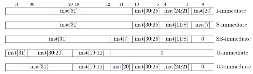
We don't specify an encoding for ImmSel (i.e. you need to design one yourself!), but make sure that your Immediate Generator and Control Logic use the same values for ImmSel.
To edit this subcircuit, edit the imm-gen.circ file and NOT the imm_gen in cpu.circ. Note that if you modify imm-gen.circ, you will need to close and re-open cpu.circ to load the changes in your CPU.
Again, here's a quick summary of its inputs and outputs:
| Signal Name | Direction | Bit Width | Description |
|---|---|---|---|
| inst | Input | 32 | The instruction being executed |
| ImmSel | Input | 3 | Value determining how to reconstruct the immediate |
| imm | Output | 32 | Value of the immediate in the instruction |
Info: Control Logic
The Control Logic unit (control-logic.circ) provided in the skeleton is based on the control logic unit in the 5-stage CPU used in lecture and discussion. In order to correctly identify each instruction, control signals play a very important part in this project. However, figuring out all of the control signals may seem intimidating. We suggest taking a look at the lecture slides and discussion worksheets to get started. Try walking through the datapath with different types of instructions; when you see a MUX or other component, think about what selector/enable value you will need for that instruction.
You are welcome to add more inputs or outputs to the existing starter control_logic circuit as your control logic demands. You may also use as many or as few of the supplied ports as needed. That being said, please DO NOT edit, move, or remove any of the existing ports during this process.
There are a two major approaches to implementing the control logic so that it can extract the opcode/funct3/funct7 from an instruction and set the control signals appropriately.
-
The recommended method is hard-wired control, as discussed in lecture, which is usually the preferred approach for RISC architectures like MIPS and RISC-V. Hard-wired control uses various gates and other components (remember, we've learned how components like MUXes can be built from AND/OR/NOT gates) to produce the appropriate control signals.
-
The other way to do it is ROM control. Every instruction implemented by a processor maps to an address in a Read-Only Memory (ROM) unit. At that address in the ROM is the control word for that instruction. Finally, the control word is broken down to individual control signals. This approach is common in CISC architectures like Intel's x86-64, and, in real life, offers some flexibility because it can be re-programmed by changing the contents of the ROM.
To edit this subcircuit, edit the control-logic.circ file and not the control_logic in cpu.circ. Note that if you modify this circuit, you will need to close and re-open cpu.circ to load the changes in your CPU.
Tips
-
If you're a spreadsheet kind of person, a spreadsheet might help you organize your control logic!
-
Hard-wired control: for signals like ALUSel, where you might want to output a certain number depending on multiple potential input signals, a Priority Encoder might be helpful!
Example
Let's consider a toy example of an ALU that only performs 3 operations: add (ALUSel=0), mul (ALUSel=1), and `sub` (ALUSel=2). Suppose that we haveis_<operation>tunnels that tell us whether an instruction requires the ALU to perform that operation. To generate the ALUSel control signal, we can simply connect eachis_<operation>tunnel to its corresponding ALUSel position (say position 2 for sub) on the Priority Encoder. Now, the Priority Encoder will return the position of the active input signal, which in this case is the correct ALUSel value.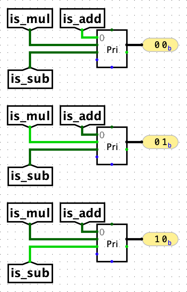
Note: In case there are multiple active signals at the same time, a Priority Encoder returns the largest active position. However, you should try to avoid having multiple active signals at once for this use case. After all, a single instruction can't require the ALU to perform both add and multiply at once.
Info: Memory
The Memory unit (located in mem.circ) represent the Data Memory of your CPU. It is already fully implemented for you and attached to the outputs of your CPU in cpu-harness.circ! You must not add mem.circ into your CPU; doing so will cause the autograder to fail and you will not receive a score.
Here's a quick summary of its inputs and outputs:
| Signal Name | Direction | Bit Width | Description |
|---|---|---|---|
| WriteAddr | Input | 32 | Address to read/write to in Memory |
| WriteData | Input | 32 | Value to be written to Memory |
| Write_En | Input | 4 | The write mask for instructions that write to Memory and zero otherwise |
| CLK | Input | 1 | Driven by the clock input to the CPU |
| ReadData | Output | 32 | Value of the data stored at the specified address |
-
Due to Logisim limitations, only the lower 16 bits of the memory address are used, and the upper 16 bits are discarded. Therefore, memory (IMEM and DMEM) in this project has an effective address space of 2^16 byte addresses.
-
While the address you give to memory is a byte address, the memory unit returns an entire word. The memory unit ignores the bottom two bits of the address you provide to it, and treats its input as a word address rather than a byte address. For example, if you input the 32-bit address 0x0000_1007, it wil be treated as the word address 0x0000_1004, and the output will be the 4 bytes at addresses 0x0000_1004, 0x0000_1005, 0x0000_1006, and 0x0000_1007.
-
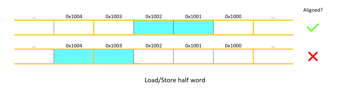
Note that for the
lh,lw,sh,swinstructions, the RISC-V ISA supports unaligned accesses, but implementing them is complicated. We'll only be implementing aligned memory accesses in this project. This means that operations will only be defined when they do not exceed the boundaries of a contiguous word in memory. An example of such an operation is anylworswthat operates on an address that is a multiple of 4. Since the address is a multiple of 4 and we load 4 bytes in a word, the total memory fetched does not exceed the boundaries of a contiguous word in memory. You must not implement unaligned accesses; you would likely need to use stalling, which would result in your output not matching our expected output (bad for your score).Another example of aligned and unaligned memory accesses.
-
You might find it helpful to review (former TA) Ryan Lund's notes on how memory works in Project 3.
-
Remember that the memory is also byte level write enabled. This means that the Write_En signal is 4 bits wide and acts as a write mask for the input data (i.e. each bit of the mask enables writing to the corresponding byte of the word). Some examples (W = byte will be overwritten, blank = byte is unaffected):
| Inst | Write_En | Byte 3 | Byte 2 | Byte 1 | Byte 0 (least significant) |
|---|---|---|---|---|---|
| sb | 0b0001 | W | |||
| sb | 0b0010 | W | |||
| sb | 0b0100 | W | |||
| sb | 0b1000 | W | |||
| sh | 0b0011 | W | W | ||
| sh | 0b0110 | W | W | ||
| sh | 0b1100 | W | W | ||
| sw | 0b1111 | W | W | W | W |
| non-store | 0b0000 |
- The ReadData port will always return the value in memory at the supplied address, regardless of Write_En.
Info: Control Status Registers (CSRs)
In order to run the testbenches that determine your project grades, there are a few more instructions that need to be added. A Control Status Register (CSR) holds additional information about the results of machine instructions, and it usually is stored independently of the register file and the memory. In your processor, you will be writing outputs to one of the CSRs that will be monitored by more complex testbenches.
Below are the 2 CSR instructions that you will need to implement. Note that while there are 2^12 possible CSR addresses, we only expect one of them to work (tohost = 0x51E). Writes to other CSR addresses should not affect the tohost CSR.
csrw tohost, rs1(short forcsrrw x0, csr, rs1wherecsr=tohost=0x51E)csrwi tohost, uimm(short forcsrrwi x0, csr, uimmwherecsr=tohost=0x51E)
The instruction formats for these instructions are as follows:
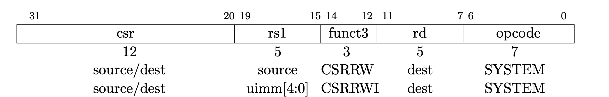
Note that the immediate forms use a 5-bit zero-extended immediate (uimm) encoded in the rs1 field.
The Control Status Registers unit (located in csr.circ) is already fully implemented for you! Please do NOT edit anything in the circuit, including input/output pins, or the autograder tests may fail.
However, you MUST include the csr subcircuit in your main CPU circuit and connect it appropriately.
Here's a quick summary of its inputs and outputs:
| Signal Name | Direction | Bit Width | Description |
|---|---|---|---|
| CSR_address | Input | 12 | Input CSR register address |
| CSR_din | Input | 32 | Value to write into specified CSR register |
| CSR_WE | Input | 1 | Write enable |
| clk | Input | 1 | Clock input |
| tohost | Output | 32 | Output of the tohost register |
While it is absolutely not required for this project, if you want to learn more about CSRs, you can refer to the RISC-V unprivileged specification (Chapter 10 in draft 2021-06-12).
Info: Processor
The main CPU circuit (located in cpu.circ) implements the main datapath and connects all the subcircuits (ALU, Branch Comparator, Control Logic, Control Status Registers, Immediate Generator, Memory, and RegFile) together. After finishing this task, your CPU should be making use of all these components.
As a refresher, here's a quick summary of its inputs and outputs:
| Input Name | Bit Width | Description |
|---|---|---|
| READ_DATA | 32 | Driven with the data at the data memory address identified by the WRITE_ADDRESS (see below). |
| INSTRUCTION | 32 | Driven with the instruction at the instruction memory address identified by the FETCH_ADDRESS (see below). |
| CLOCK | 1 | The input for the clock. As with the register file, this can be sent into subcircuits (e.g. the CLK input for your register file) or attached directly to the clock inputs of memory units in Logisim, but should not otherwise be gated (i.e., do not invert it, do not AND it with anything, etc.). |
| Output Name | Bit Width | Description |
|---|---|---|
| ra | 32 | Driven with the contents of ra (FOR TESTING) |
| sp | 32 | Driven with the contents of sp (FOR TESTING) |
| t0 | 32 | Driven with the contents of t0 (FOR TESTING) |
| t1 | 32 | Driven with the contents of t1 (FOR TESTING) |
| t2 | 32 | Driven with the contents of t2 (FOR TESTING) |
| s0 | 32 | Driven with the contents of s0 (FOR TESTING) |
| s1 | 32 | Driven with the contents of s1 (FOR TESTING) |
| a0 | 32 | Driven with the contents of a0 (FOR TESTING) |
| tohost | 32 | Driven with the contents of CSR 0x51E (FOR TESTING) |
| WRITE_ADDRESS | 32 | This output is used to select which address to read/write data from in data memory. |
| WRITE_DATA | 32 | This output is used to provide write data to data memory. |
| WRITE_ENABLE | 4 | This output is used to provide the write enable mask to data memory. |
| PROGRAM_COUNTER | 32 | This output is used to select which instruction is presented to the processor on the INSTRUCTION input. |
We strongly recommend that you review the Single Stage CPU: A Guide section from Part A.
Note that you must modify your write back phase by inserting a MUX between the Register File and the outputs from the:
- ALU
- MEM (`READ_DATA1)
- PC+4 (think about which isntructions use this) The WBSel control signal is used to select the correct output to the Register File.
Again, make sure that you do not edit the input/output pins or add new ones!
Notices
- To prevent double jeopardy, the autograder will replace your ALU and RegFile with the staff ALU and RegFile. This means that if your ALU or RegFile from Part A have issues, they will not affect your autograder results in Part B. However, this also means that you must not depend on out-of-spec behavior from these circuits.
Single-Cycle CPU Testing
We've provided some basic sanity tests for your CPU in the tests/part-b/sanity/ directory. You can run these with:
$ python3 test.py tests/part-b/sanity/
Refer to the Info: CPU Testing section from Part A for more info on using these tests.
Note that these sanity tests are not comprehensive; they are intended to guide you in the early stages of testing until you start Task 6.
Task 6: Custom Tests
For Part B, we have provided a set of sanity tests in the starter code. These tests are meant to help reduce your stress by providing some guidance in the early stages of testing, but they are not comprehensive. You should still write rigorous tests for your designs, as passing the basic sanity tests does not guarantee that you will pass any of the hidden tests.
The autograder tests for Part B fall into 3 main categories: visible unit tests, visible integration tests, and hidden edge case tests.
However, we're revealing the names of the hidden edge case tests to help you re-create a close approximation of them with the tools we provide.
Unit tests: A unit test exercises your datapath with a single instruction, to make sure that each individual instruction has been implemented and is working as expected. You should write a different unit test for every single instruction that you need to implement, and make sure that you test the spectrum of possibilities for that instruction thoroughly. For example, a unit test slt should contain cases where rs1 < rs2, rs1 > rs2, and where rs1 == rs2.
Integration tests: After you've passed your unit tests, move onto tests that use multiple functions in combination. Try out various simple RISC-V programs that run a single function; your CPU should be able to handle them, if working properly. Feel free to try to use riscv-gcc to compile C programs to RISC-V, but be aware of the limited instruction set we're working with (you don't have any ecall instructions, for example). We'd recommend that you instead try to write simple functions on your own based on what you've seen in labs, discussions, projects, and exams.
Edge case tests: Edge case tests try inputs that you normally wouldn't expect, which may trigger bugs in certain situations. What edge cases should you look for?
Here's a list of their names:
- Branching: Overgrown Tree Edition
- Immediates: Extra-Strength 0xC0FFEE
- Jumping: Hop-Hop-Hopscotch
- Jumping: Into NOPe-land!
- Jumping: The Far Lands
- Memory: Siiiiiiiign Extension
- Memory: When The Planets Don't Align
- Registers: Try Them All!
- Loading: Lots of LUIve
Creating Custom Tests
Here's a companion video that goes with this section.
We've included a script (tools/create-test.py) that uses Venus to help you generate test circuits from RISC-V assembly! The process for writing custom tests is as follows:
- Come up with a test, and write the RISC-V assembly instructions for that test, saving them in a file ending in
.sin thetests/part-b/custom/inputs/folder. The name of this file will be the name of your test. Repeat if you have more tests.
-
e.g.
tests/part-b/custom/inputs/sll-slli.sandtests/part-b/custom/inputs/beq.sNote: IMEM and DMEM are separate in Logisim, but combined in Venus. This means that if you write assembly code that tries to access memory overlapping with instructions, Venus will throw an error. Since counting exactly how many instructions your assembly code requires, and multiplying that by 4 can be annoying, we suggest you load/store using addresses greater than 0x3E8 (leaving space for 1000 bytes/250 instructions), and increase this offset if you have more instructions.
- Generate the test circuits for your tests using
create-test.py:
$ python3 tools/create-test.py tests/part-b/custom/inputs/sll-slli.s tests/part-b/custom/inputs/beq.s
Reminder: if you want to regenerate everything, you can take advantage of Bash globs:
$ python3 tools/create-test.py tests/part-b/custom/inputs/*.s
This should generate a couple new files to go with your assembly file:
tests/part-b/custom/:
  - cpu-<TEST_NAME>.circ                                # The new circuit for your test
  - inputs/<TEST_NAME>.s                                # The test file you wrote (unchanged)
  - reference-outputs/cpu-<TEST_NAME>-pipelined-ref.out # The pipelined reference output for your test
  - reference-outputs/cpu-<TEST_NAME>-ref.out           # The single-cycle reference output for your test
- Now you can run the tests you just wrote!
$ python3 test.py tests/part-b/custom/sll-slli.circ tests/part-b/custom/beq.circ
Reminder: you can run all tests in a directory:
$ python3 test.py tests/part-b/custom/
By default, the number of cycles for a test will be just enough for all instructions in the test, as well as extra cycles for the register writeback and pipelining. If you wish to override this and simulate your code for a certain number of cycles, you can use the --cycles flag:
$ python3 tools/create-test.py --cycles <NUMBER_OF_CYCLES> <ASM_PATH>
Refer to the Info: CPU Testing section for more info on using these tests.
Test Coverage
Test Coverage: a metric measuring how much of a codebase is being tested by tests. For the purposes of this project, you will be graded on how much of the required ISA your tests cover.
The autograder for Part B will examine the coverage of tests located in the tests/part-b/custom/inputs/ folder. When you submit Part B to the autograder, the autograder will output a message about the percentage coverage of your tests against our staff suite of tests and notify you if any of your tests raised a syntax error.
Coverage Hints
- If you make many short test files rather than one large one, it will be easier to figure out which test and which line causes your Syntax Error (and to figure out where your CPU is failing). We'd recommend that for unit testing, where you have one
.sfile testing each instruction. - Make sure you test every single instruction in the ISA, including the ones that are covered by the sanity tests; feel free to use the sanity tests as a model or even incorporate them as part of your test suite.
- Make sure you check that all registers are working.
- Make sure you don't have any "dummy" tests; if a test doesn't lead to a change in state or register value, it is not a meaningful test. For example, loading the value 0 from memory into a register that already has the value of 0 doesn't change the value in the register, so you can't determine if the load instruction actually worked or not by looking at the test output.
- Make sure your tests accumulate outputs into the special registers we have debug outputs for, as other registers cannot be directly checked (reminder:
ra,sp,t0,t1,t2,s0,s1, anda0). - Consider if an instruction uses a signed or unsigned immediate. How would you test for implementations using the wrong sign?
Notices
- Most instructions use registers or memory. In order to test these instructions, we need to load different values into registers and memory, which we (currently) unavoidably have to do using
addi,lui, andsw. This means that your CPU must handleaddiandluiproperly, or they may cause other instructions' tests to fail. Additionally, failures inlworswmay affect each other, since we (currently) cannot write to memory withoutswor inspect a value in memory withoutlw. Make sure to test these instructions extensively! - Venus does not support CSRs, so you will not be able to generate custom tests for CSR-related instructions (e.g.
csrw,csrwi). To compensate, the autograder has a visible robust CSR test that will test all needed functionality of the CSR. - You can create custom tests with pseudoinstructions and run them locally, but the Test Coverage autograder does not currently support them, so pseudoinstructions won't count toward your coverage statistics.
- Avoid creating tests that use out-of-range memory addresses (2^16 and above) or memory addresses that aren't valid for that load/store instruction (see the Memory section in Task 5). Venus supports these, so the tests will be generated, but your CPU should not, so your CPU will not be able to pass these tests.
Task 7: Pipelining
So far, your CPU is capable of executing instructions in our ISA in a single cycle. Now, it's time to implement pipelining in your CPU! For this project, you'll need to implement a 2-stage pipeline, which is still conceptually similar to the 5-stage pipeline covered in lecture and discussion (review those if you need a refresher). The two stages you'll implement are:
- Instruction Fetch: An instruction is fetched from the instruction memory.
- Execute: The instruction is decoded, executed, and committed (written back). This is a combination of the remaining four stages of a classic five-stage RISC-V pipeline (ID, EX, MEM and WB).
Because all of the control and execution is handled in the Execute stage, your processor should be more or less indistinguishable from a single-cycle implementation, barring the one-cycle startup latency. However, we will be enforcing the two-stage pipeline design. Some things to consider:
- Will the IF and EX stages have the same or different
PCvalues? - Do you need to store the
PCbetween the pipelining stages? - What hazards are present in this two-stage pipeline?
You might also notice a bootstrapping problem here: during the first cycle, the instruction register sitting between the pipeline stages won't contain an instruction loaded from memory. What should the second stage do? Luckily, Logisim automatically sets registers to zero on reset, so the instruction pipeline register will automatically start with a nop! If you wish, you can depend on this behavior of Logisim.
Control Hazards
Since your CPU will support branch and jump instructions, you'll need to handle control hazards that occur when branching.
-
The instruction immediately after a branch or jump should not be executed if a branch is taken. This makes your task a bit more complex. By the time you have figured out that a branch or jump is in the execute stage, you have already accessed the instruction memory and pulled out (possibly) the wrong instruction. Therefore, you will need to flush the instruction that is being fetched (next instruction) if the instruction under execution (current instruction) is a taken branch or jump.
-
Instruction flushing for this project MUST be accomplished by MUXing a
nopinto the instruction stream and sending thenopinto the Execute stage instead of using the fetched instruction. You can useaddi x0, x0, 0(0x00000013), for this purpose; othernopinstructions will work too. You should flush only if a branch is taken (do not flush if it is not taken). You should always flush the next instruction when jumping. -
Note: you should not solve this issue by calculating branch offsets in the IF stage. We compare your output against a reference output that uses
nop, so a solution that doesn't usenopmay not match the reference output even if it is a conceptually correct solution.
Some more things to consider:
- To MUX a
nopinto the instruction stream, do you place it before or after the instruction register? - What address should be requested next while the EX stage executes a
nop? Is this different than normal?
Pipelined CPU Testing
We've provided some basic sanity tests for your pipelined CPU in the tests/part-b/sanity/ directory (same tests as in Task 6). You can run these with:
$ python3 test.py --pipelined tests/part-b/sanity/
Note: since your CPU is pipelined at this point, you need to run the pipelined tests using the --pipelined (or -p) flag. If you run the single-cycle tests (i.e. omit the --pipelined flag) after pipelining your CPU, your CPU should now fail those tests! Think about why this happens...
Similarly, you can also run the pipelined version of your custom tests:
$ python3 test.py --pipelined tests/part-b/custom/
Note: because you're implementing a 2-stage pipelined processor and the first instruction writes on the rising edge of the second clock cycle, the effects of your instructions will have a 2 instruction delay. For example, let's look at the first instruction of tests/part-b/sanity/inputs/addi.s, addi t0, x0, -1. If you inspect the pipelined reference output (tests/part-b/sanity/reference-output/cpu-addi-pipelined-ref.out), you'll see that t0 doesn't show changes until the third cycle.
Refer to the Info: CPU Testing section for more info on using these tests. Keep in mind that you're working with a pipelined circuit from this task onward.
Task 8: Part B README Update
Time to update your README.md! Once again, write down how you implemented your circuits and components for this part (including the various subcircuits you used), and explain the reasoning behind your design choices. In particular, we want to see:
- How you designed your control logic
- Advantages/Disadvantages of your design
- Best/Worst bug or design challenge you encountered, and your solution to it
Your additions to the README should be at least 512 characters (although something more than the bare minimum would be nice), but other than that feel free to get creative!
Submission
At this point, if you've completed tasks 5-8, you've finished Part B of the project. Congratulations on your shiny new CPU!
Double-check and make sure that that:
- You have not moved any provided input/output pins, and that your circuits fit in the provided testing harnesses
- You did not create any additional
.circfiles; the autograder will only be testing the circuit files you were allowed to edit for Part B (branch-comp.circ,control-logic.circ,cpu.circ,imm-gen.circ). - Your custom
.stests are located intests/part-b/custom/inputs/, since the autograder will test those for coverage. - You have completed Task 8 (README update)
To prevent double jeopardy, the autograder will replace your ALU and RegFile with the staff ALU and RegFile. This means that if your ALU or RegFile from Part A have issues, they will not affect your autograder results in Part B. However, this also means that you must not depend on out-of-spec behavior from these circuits.
The autograder for Part B uses the sanity tests provided in the starter code, as well as hidden unit, integration, and edge case tests as specified in Task 6. Additionally, the autograder will check your custom tests for test coverage.
Note: If you fail on any of the provided autograder sanity tests, course staff will not help you debug your CPU unless you have recreated the failure in a custom test.
Grading
Part B is worth 80% of your overall Project 3 grade. The grading breakdown is as follows:
- Sanity and Visible Unit Tests (44%)
- Visible Integration Tests (5%)
- Hidden Edge Case Tests (20%)
- Test Coverage (10%)
- README (1%)