We are about to descend to the circuit level, in preparation for examining the central processing unit and other computer components. Integrated circuits are laid out on a bare die that's primarily crystalline silicon. The width and length of the die range from 1 to 25 millimeters. There are roughly 100 million to a billion transistors on the die, each around 65 nanometers (65 × 10-9 meters) in size. They are organized into logic gates, roughly four transistors per gate; the die thus contains between 25 to 100 million gates. There are several conductive layers on the die in which signals travel from place to place on the die.
A chip contains a die, mounted on a ceramic or plastic base. The connections on the die are much too close together to be accessible from outside the die, so the ceramic base provides a way of spreading them out. It also allows heat to be dissipated. (Power consumption and the resulting generation of heat are the big constraints on performance.)
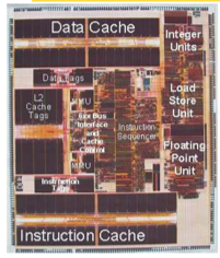
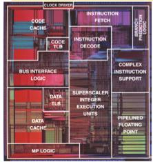
A couple of examples of real dies appear below. One is a relatively old (late 1990's) PowerPC; the other is a more recent Pentium.
Labels on the photographs identify functional units on the dies:
In two or three weeks, we will see how all these units are organized. For example, the MIPS CPU is diagrammed below.
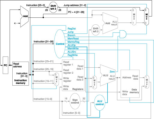
Its building blocks—adders, multipliers, shifters, and selectors—are all made of the logic gates that we'll shortly be studying.
Any circuit has one or more inputs and one or more outputs. In a combinational logic circuit, the output values are based entirely on the input values. A state element, on the other hand, has memory; its outputs are based not only on the current input values but on earlier inputs as well. We'll study state elements in the next lab. Here we focus on combinational circuits. They are like mathematical functions - the output depends soley on the input, and there is a beautiful body of theory and practice.
The digital abstraction allows us to treat a certain voltage range as representing the logical value 1 or TRUE and below this the value 0 or FALSE. In your electical engineering courses you will learn how to construct circuits that take these digital values as inputs and produce digital values as outputs. In cs61cl, we work at the digital abstraction - and it is beautiful.
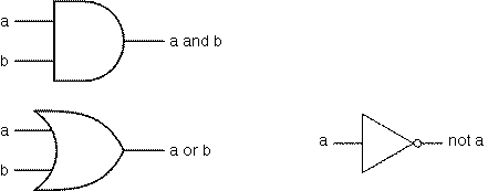
A circuit is built of gates and wires. The typical gates that you'll recognize from logic are "and", "or", and "not"; outputs from gates can be connected by wires as inputs to other gates to construct more complex functions from simpler ones. We will shortly see how to construct more complicated circuits out of these three primitives. Right now, we will look at three ways of representing a circuit.
For each pattern of 1's and 0's in the inputs to a combinational logic circuit, there is a unique output value. A truth table lists all the possible input values along with the corresponding output values. There is a column in the table for each input and for each output. There is a row in the table for each pattern of 1's and 0's in the input. Listed below as examples are the truth tables for "and", "or", and "not"; in each case, the inputs are designated by a and b and the output by c.
| and | or | not |
a b a and b 0 0 0 0 1 0 1 0 0 1 1 1 |
a b a or b 0 0 0 0 1 1 1 0 1 1 1 1 |
a not a 0 1 1 0 |
A circuit can also be represented graphically with a symbol. The conventional graphical representations for "and", "or", and "not" are shown below. Graphical structures convenient for conveying the structure of a circuit. The set of logic gate symbols are standardized and used internationally. We'll show you the others later. The little circle on the end of a wire indicates negation.
Finally, a circuit can be represented algebraically using Boolean algebra. Boolean variables, as you know from programming, can take on two values, true and false. We will use the operator "⋅" for "and", "+" for "or", and "!" for "not". (The readings use an overbar for "not", but we are unaware of any way to apply an overbar to a character or expression in HTML.) An example expression would then be
a ⋅ (!b + c)
which is read as "a and the quantity not b or c".
a b c 	out
0 0 0 	1
0 0 1	1
0 1 0	1
0 1 1	1
1 0 0	1
1 0 1	1
1 1 0	1
1 1 1	1
Notice how you have covered all the possible inputs? It is all the n-bit values from 0 to 2^n - 1 in order.
The "exclusive or" function ("xor") is a very useful digital logic gate and you have already used the xor operator in C '^'. We'll construct it out of the gates we have seen so far and illustrate all three representations. The "xor" of two boolean values is 1 if one of the values is 0 and the other is 1, and 0 otherwise. This informal description is made precise in the truth table.
    a    b    a xor b
    0    0       0
    0    1       1
    1    0       1
    1    1       0
An algebraic expression defining the "xor" operator is
x = a ⋅ !b + !a ⋅ b
Finally, this expression can be represented a ciruit of gates and wires as follow. This graphical representation is called a schematic.
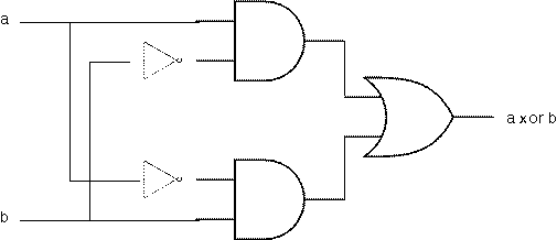
Note that each of the inputs a and b is wired as input to two gates. This "forking" of input values is quite common.
The xor is so important that it has its own logical symbol.

 .
.
a b	a nand b
0 0	1
0 1	1
1 0	1
1 1	0
Give a definition of nand in a simple sentence.
The Logisim program provides a way to build, visualize, and simulate circuits. The technical term for this kind of tools is "schematic capture". (In the old days we had little plastic templates and would trace the outlines of logic symbols on paper and draw lines to wire them up - just like drafting the design of a house. Computer Aided Design (CAD) tools, like those invented at Berkeley allowed you to "capture" these designs in a machine readable. In CS150 and CS152 we use professional tools for this. But, they have a huge learning curve and lots of company specific features. Logisim is a very basic tool, but it is quick to learn, easy to use and just enough for our needs.) Run it by ssh'ing to cory.eecs as you did to use MARS. Then type
java -jar ~cs61c/bin/logisim.jar
or merely
logisim
to the UNIX prompt. You can learn about Logisim beyond the scope of this lab (or download it to use at home) from the Logisim website.
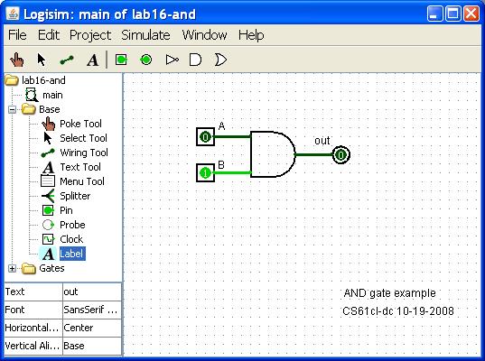
Start by creating a very simple circuit just to get the feel for placing gates and wires.
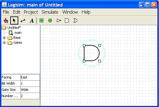
Click the "AND gate"  button in the toolbar above the layout area.
This will cause the shadow of an AND gate to follow your cursor around.
Click once within the main schematic window to place an AND gate.
In the little description in the lower left portion of the window, adjust the
number of inputs to 2. Notice the orientation is Facing East. With more complex designs you will need to take care in how you place things on the page.
So far it looks like
button in the toolbar above the layout area.
This will cause the shadow of an AND gate to follow your cursor around.
Click once within the main schematic window to place an AND gate.
In the little description in the lower left portion of the window, adjust the
number of inputs to 2. Notice the orientation is Facing East. With more complex designs you will need to take care in how you place things on the page.
So far it looks like
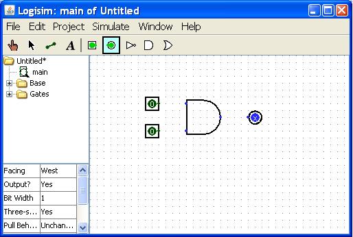
Click the "Input Pin"  button. Now, place two input pins somewhere to the left of your AND
gate so they line up with the little dots on the gate.
button. Now, place two input pins somewhere to the left of your AND
gate so they line up with the little dots on the gate.
Click the "Output Pin"  button.
Then place an output pin to the right of your AND gate. Your schematic should look something like this at this point:
button.
Then place an output pin to the right of your AND gate. Your schematic should look something like this at this point:
 Click and drag to connect the input pins to the little dots on the left side of the AND gate.
This may take several steps, as you can only draw vertical and horizontal wires. Just draw a wire horizontally, release the mouse button, then click and drag down starting from the end of the wire to continue vertically.
You can attach the wire to any pin on the AND gate on the left side. Repeat the same procedure to connect the output (right side) of the AND gate to the output pin. After completing these steps your schematic should look roughly like this:
Click and drag to connect the input pins to the little dots on the left side of the AND gate.
This may take several steps, as you can only draw vertical and horizontal wires. Just draw a wire horizontally, release the mouse button, then click and drag down starting from the end of the wire to continue vertically.
You can attach the wire to any pin on the AND gate on the left side. Repeat the same procedure to connect the output (right side) of the AND gate to the output pin. After completing these steps your schematic should look roughly like this:
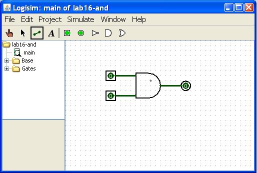
 tool and try clicking on the input pins in your schematic. Observe what happens, verifying that this circuit does what you think an AND gate should do. Compare this to
the truth table for AND.
tool and try clicking on the input pins in your schematic. Observe what happens, verifying that this circuit does what you think an AND gate should do. Compare this to
the truth table for AND.
In C and Java programs we tackle hard problem by divide a conquer. We build helper functions to solve subproblems and then put them together to solve the whole problem. Good design means managing complexity. The same is true for logic design. A schematic can contain subcircuits. Here, we will create a subcircuit to demonstrate its use.
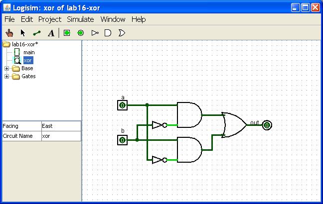
Start by creating a new schematic for your work (File->New), then a new subcircuit (Project->Add Circuit ). You will be prompted for a name for the subcircuit; call it "XOR". In the new schematic window that you see create a simple xor circuit with 2 input pins on the left side and an output pin on the right side. Go back to your "main" schematic by double-clicking "main" in the circuit selector at the left of the screen. Your original (blank) schematic will now be displayed, but your xor circuit has been stored. Now, single-click the word "XOR" in the list. This will tell Logisim that you wish to add your "XOR" circuit into your "main" circuit.
Try placing your XOR circuit into the "main" schematic. If you did it correctly, you should see a gate with 2 input pins on the left and one output pin on the right. Try hooking input pins and output pins up to these and see if it works as you expect.It should look something like this.
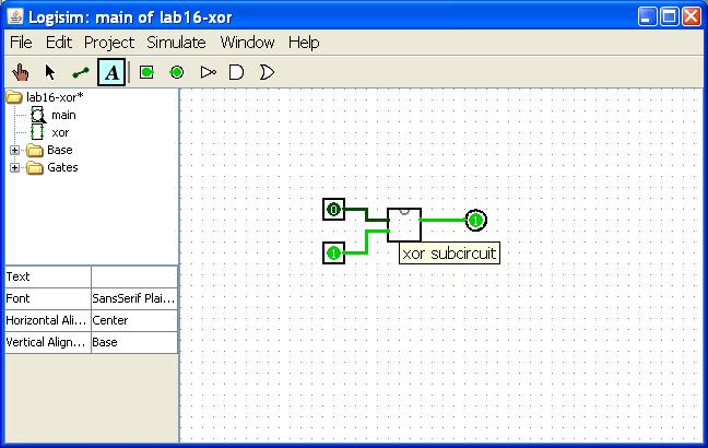
Now lets instantiate this subcircuit in out main schematic. Double click on main to make it the focus. Now add an XOR subcircuit by clicking and dropping, just like you did a gate. Notice the two dots on the left side. That's where we put the input pins. The one on the right is the output pin. You need to be extremely careful in logisim with the placement of pins in you subcircuits.
Hook up inputs and output so that you can try out your new hierarchical circuit. Now you can poke the inputs and see that this is indeed an xor. It should look something like this.
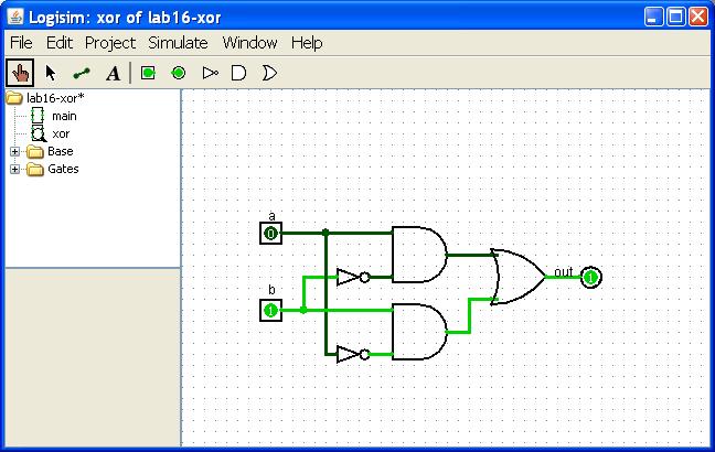
In debugging you need to be able to work up and down the abstractions that you build. Here it is subcircuits. ctrl-click on the xor symbol should pop-up a view xor option. Selecting that takes you into the xor circuit with the input values being the ones that are present in the main circuit. In our case, it looks like this.
One thing about hardware - it is inherently parallel. Everything in the circuit is happening at once. Subcircuits are note "invoked" like functions and proceedures in a programming language - they exist in hardware. In simulation, they behave like the actual hardware - it all exists. In fact, let's go back to the main circut and drop in another xor and another input, so it looks like this.
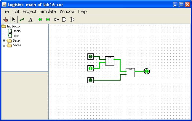
This is an "odd parity" circuit. It's output is 1 when the number of inputs with value 1 is odd. Try poking its inputs. View the underlying subcircuits. See how they are different? You can use the Simulate pull-down to navigate up and down.
"Give me a lever and I'll lift the world." Now that we can build big circuits by composing smaller ones, we can build anything. (Well, almost. We still only have combinational elements. We'll need some state too.)
Consider a 1-bit adder that produces a 2-bit result: 0 + 0 = 00, 0 + 1 = 1 + 0 = 01, and 1 + 1 = 10. Let a and b be the bits to be added, with s1 being the leftmost (most signficant) bit of the sum, and s0 the rightmost bit of the sum.
Construct the truth table. Hint: It should have four columns and four rows.
Identify an expression for s1.
Do the same for s0, the least signficant bit of the sum.
Create a new project. The circuit described above has a name; it is called a "Half Adder". We'll see a full adder later. Add a subcircuit called HA that implements the 1-bit adder in Logisim as a subcircuit. Can use your XOR subcircuit.
Also implement the following function that would be part of a "mod 4" counter. The combinatorial logic circuit within the counter would take a 2-bit value as input and produce a 2-bit output representing the next value in the sequence 00, 01, 10, 11, 00, 01, 10, 11, 00, ... Use the xor gate in your solution. Start by writing down the truth table. Express each output as a function of the two inputs.
Starting from a truth table, we can write a special Boolean expression that matches its behavior, namely the sum-of-products canonical form. ("Canonical Form" is an important concept in EECS that shows up wherever you have many ways of representing the same thing. You probably encountered it first in grade school where you "simplified factions" by all common divisors in the numerator and demoninator. Of course, each rational number has an infinite number of ways it can be represented as a fraction, but this one is unique. You see the same thing in writing polynomials in stardard form with exponent decreasing to the right. You saw it with normalized floating point numbers.) The sum-of-products (SOP) expression is the OR of a set of terms, each term being a product (AND) of input variables or their complements. Every row where 1 appears in the output contributes a term in the Boolean expression. Each AND term includes all the input variables in either complemented or uncomplemented form. A variable appears in complemented form if it is a 0 in the row of the truth table, and uncomplemented if it appears as a 1 in the row.
Here's an example of producing the sum-of-products form for a three-input function.
| min term | a b c | y |
| 0 0 0 | 0 | |
| !a ⋅ !b ⋅ c | 0 0 1 | 1 |
| !a ⋅ b ⋅ !c | 0 1 0 | 1 |
| 0 1 1 | 0 | |
| a ⋅ !b ⋅ !c | 1 0 0 | 1 |
| 1 0 1 | 0 | |
| 1 1 0 | 0 | |
| a ⋅ b ⋅ c | 1 1 1 | 1 |
The sum-of-products expression is
y = !a ⋅ !b ⋅ c + !a ⋅ b ⋅ !c + a ⋅ !b ⋅ !c + a ⋅ b ⋅ !c
This sum-of-products can be implemented directly in gates or it can be simplified further. (By the way, does this look familiar? Do you see any use for it?)
A Full Adder (FA) is a circuit that takes three inputs, a and b, as well as a carry in, cin. It implements (in binary) the addition step that you learned as a child - sum the carry-in (that you wrote at the top of the column) and the two input values to produce a sum (in the same column) and a carry out (that you wrote on top of the next column). The FA just does one column (called a bit-slice). It generates two outputs, a sum bit, s, as well as a carry out. All of this is more precisely described by the truth table. (Note, this is really two truth tables. One for "cout" and one for "s" that are built on the same inputs.)
a b cin	cout 	s
0 0 0	0	0
0 0 1	0	1
0 1 0	0	1
0 1 1	1	0
1 0 0	0	1
1 0 1	1	0
1 1 0	1	0
1 1 1	1	1
There is a carry out if there are two or more 1's in the input. The sum is 1 if the number of 1s in the input is odd.
In logisim, start new project called adder. Add a subcircuit called FA. In that subcircuit, drop three input pins and two output pins. Pull down Project->Analyze Circuit. Click on inputs, you will see that it has named them a, b, c. Click on outputs; they are x and y. Now, click on Table. By clicking the entries in the result column, create a truth table where x is the carry out and y is the sum. It should look like this.
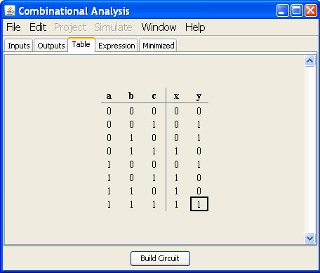
Click on the expression tag. See the logical expression for x says formally "are two of the inputs true?" and the logical expression for y says "is the number of true inputs odd?".
Now click on the Build Circuit button. It asks you for a circuit name. We could stick this in a new cubcircuit, but we'll let it go in FA. Don't check either of the options, just click OK and YES in the verification box.
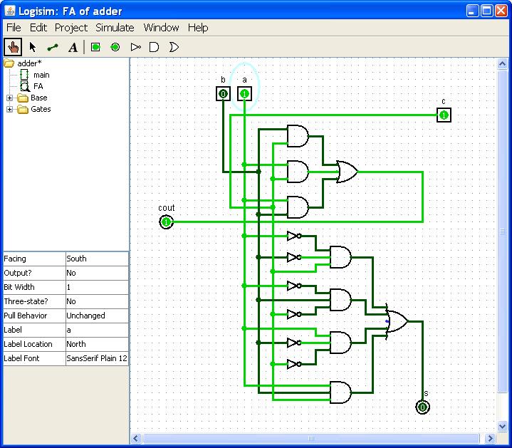
You can close this tool. Go back to the FA circuit. It now contains two beautiful SOP examples. Verify that they correspond to the logical expressions.
Using the select tool you can select a rectangular region of the circuit. Then you can move it. Clicking on a labeled pin shows its attributes in the lower left. Modify the label and the facing. So the a and b inputs are at the top facing "south". You can delete segments of wires by right-click and delete. Reconnect them so they look pretty. (In schematic capture, a bit of time in layout will save you lots of time later. Pretty circuits, pretty code, less bugs, more sleep.) Change c to be cin and put it over on the right, facing west. Change x to cout and put it in the left, facing east. Change y to s and put it on the bottom facing north. It should look like the following. Poke the inputs and convince yourself that this is an adder.
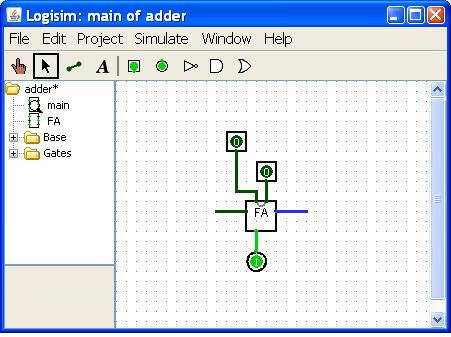
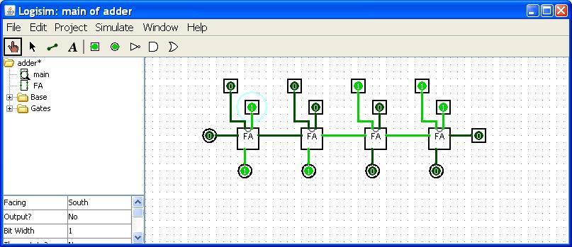
Poke at the inputs. See, it adds from left to right, just like you do, but in binary. It is called a ripple-carry adder because the carry ripples from left to right.
See the power of modular design? Imagine if you had all the gates that are inside the FA appearing in this schematic. In fact, let's go count how many there would be.
If you represented the entire 4-bit adder as a truth table, how large would it be? To check your answer, focus on the main circuit and do Project->Analyze Circuit. See, the mapping between combinational logic, truth tables and boolean expressions goes in any direction.
Congratulations, now you can design a combinational circuit for any boolean function, no matter how complex. You can define higher level building blocks, and you can compose these. From here, it is all a matter of optimization and improvement.
| i | False(i) | Identity(i) | Not(i) | True(i) |
| 0 | 0 | 0 | 1 | 1 |
| 1 | 0 | 1 | 0 | 1 |
.
And its truth table is
a   b   a nand b
0   0      1
0   1      1
1   0      1
1   1      0
Show how to build AND, OR, and NOT using only NAND. This consitutes a proof that NAND is complete.
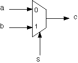
Design an implementation of a multiplexor, and add it as a subcircuit in your collection.