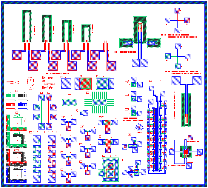
|
Label #
|
Feature Name
|
Location in Above Image
|
| 1A |
Resolution
Test Patterns (1 per mask) |
Left Center |
| 1B |
Alignment
Marks and Verniers |
Left Bottom |
| 2A |
Diffused
Resistor |
Left Center |
| 2B |
Poly
Resistor |
Left Center |
| 2C |
Metal-to-Diffusion
Contact Chain |
Left Bottom |
| 2D |
Metal-to-Poly
Contact Chain |
Left Bottom |
| 3 |
Field
Oxide Capacitor |
Center |
| 4 |
Gate
Oxide Capacitor |
Center |
| 5 |
Intermediate
Oxide Capacitor |
Center |
| 6A |
Junction
Capacitor |
Center |
| 6B |
Long
Periphery Junction Capacitor |
Center |
| 7 |
Diode |
Center |
| 8 |
MOSFETs
of various lengths |
Center Bottom |
| 9 |
Long
Channel MOSFETs |
Center Bottom |
| 10 |
Large
MOSFET |
Center Bottom |
| 11 |
Field
Oxide MOSFET |
Center Bottom |
| 12 |
Circular
MOSFET |
Center Bottom |
| 13 |
Lateral
BJTs |
Center |
| 14 |
Inverter |
Center Bottom |
| 15 |
NOR
Gate |
Center Bottom |
| 16 |
Ring
Oscillator (17 stages + buffer) |
Right Bottom |
| 17A |
Metal-Poly
Contact Resistance Test Structure |
Right Top |
| 17B |
Metal-Diffusion
Contact Resistance Test Structure |
Right Top |
| 18 |
Aluminum-SiO2
Bimorph |
Right Center |
| 19 |
Campanile |
Right Top |
| 20 |
Cantilever
Array |
Left Top |
| 21 |
Heater
Platform |
Right Bottom |
| - |
Designers'
Initials |
Center Bottom |