Name 1:
Login: ee16a-
Name 2:
Login: ee16a-
Instructions
- Complete this lab by filling in all of the required sections, marked with
"YOUR CODE HERE"or"YOUR COMMENTS HERE".
- When you finish notify your GSI to get get checked off for this lab. Be ready to answer a few questions to show your understanding of each section.
- Labs will be graded based on completion for teams of 2 students
Introduction
Welcome to the first of a series of 3 labs in the touchscreen module in which you will build 2 different touchscreen systems introduced in lecture. In the first lab we will be working with perhaps the simplest circuit that does work - an LED circuit. We will also give the circuit fading capabilities both using a physical component and using an Arduino. In the second lab, we will build a resistive touchscreen with a 3x3 grid and in the third lab we will build a single-touch capacitive touchscreen that employs a Capacitance Sharing sensing system.
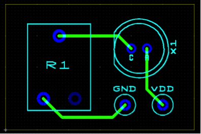
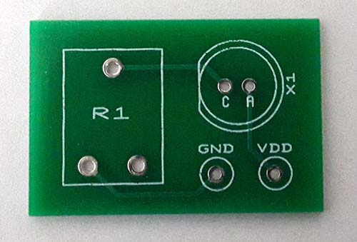
Printed Circuit Boards (PCB)

Circuit boards can be mass-produced in the form of PCBs. A PCB contains of conducting and non-conducting layers sandwiched together to connect each component to others, along with holes to fix the components to. In the diagram above, as with the PCB we will be working with today, there are only two conducting layers; more complicated PCBs may contain many more. The traces in the PCB we will actually be working on today is shown below.
Light Emitting Diode (LED)
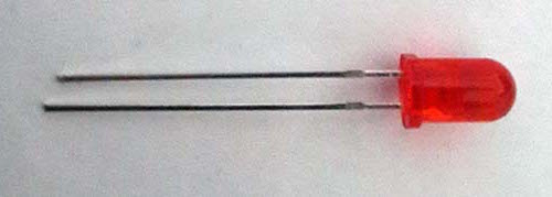
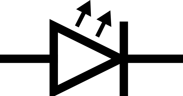
LEDs are elements that emit light when the voltage drop between its two terminals is above a certain value. Above this threshold, the LED acts as a resistor, but its resistance depends on the current forced through it. Its brightness also depends on the current flowing through the terminals. One thing to note is that the LED is a polarized device, so its two terminals are not identical. The triangular side of the LED symbol and the longer leg of the component is the positive (Anode) terminal of the device, while the flat side of the symbol and the shorter leg of the component corresponds to the negative (Cathode) terminal. In the PCB, the polarity is written as A and C respectively.
Potentiometer
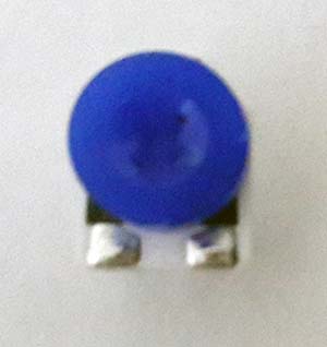

A potentiometer is a variable resistor with 3 terminals. As we turn the knob, the value of the resistance between the middle terminal and any of the other terminals change. However, the resistance between the end terminals stay constant. In this lab we will be using a 1k$\Omega$ potentiometer, whose footprint was used in designing the PCB.
Function Generator
The function generator is a useful tool that can be used to provide test inputs to your circuits. While the power supply is capable of giving you a fixed voltage, the function generator can output sine waves, square waves, and a variety of other waveforms.r/>1. Connect a probe to either the green or yellow outputs labeled "1" and "2". The function generator probes have thick wires with two smaller red and black wires exposed at one end. These correspond to positive and negative terminals respectively just like on the oscilloscope probes (e.g. for a 1V amplitude square wave the voltage difference between the red and black wires will alternate between +/- 1V).
2. Press the "Waveforms" button and select the time of waveform you'd like to output.
Just like with the oscilloscope, buttons to the right of the screen bring up menus and the buttons at the bottom of the screen allow you to select options from those menus.
3. Push the "Parameters" button and set the desired parameters for your output.
Both the number pad and the knob can be used to enter these values.
4. Press "1" or "2" corresponding to the output you have your probe connected to and then select "Output On".
The output of the function generator is off by default. When you press the button to turn it on, the corresponding "1" or "2" button shoud light up.

Task 1: LED Fader Circuit
The PCB you are given corresponds to the circuit above. Let’s analyze the circuit. Discuss the answers with a GSI. While waiting for your turn, please read on and continue to the next task.
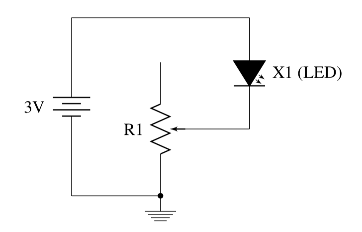
Assuming the voltage drop across X1 is 0.7V or higher, what is the relationship between the current through X1 ($I_{X1}$) and the resistance of R1. What happens to the LED when R1 is increased?
YOUR COMMENTS HERE
Can we completely turn off the LED when the power source is on? If so, how? Otherwise, why not?
YOUR COMMENTS HERE
Task 2: Building the Circuit
Materials
- PCB
- LED
- 1k$\Omega$ resistor
Now that we understand the circuit, we can start building it.
In order to build our circuit we first need to learn an important skill, soldering. Soldering is a process in which two or metal elements are joined together by melting and flowing solder into a joint, see more at http://en.wikipedia.org/wiki/Soldering. It is akin to welding, but on a much smaller scale. Soldering is useful because it enables us to establish an electrical connection between two circuit elements, which gives us the ability to build a complete circuit.
Important names and labels:
The Soldering Iron is the pencil shaped tool that is used to apply heat.
Solder is the metal filament that gets melted by the soldering iron and fills the gap between two circuit components.
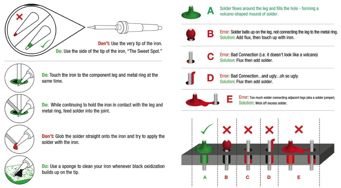
Soldering steps (repeat these steps for each joint):
- Place your desired circuit element into the PCB. We typically place our solder joints underneath our circuit elements, so make sure there is an exposed metal ring surrounding the desired joint on the side of PCB opposite the side the element is resting on. Bend the component lead around 45 degrees to fix it in place.
- Melt a small blob of solder on the tip of the soldering iron. This is called “tinning the tip” and it improves the transfer of heat from your soldering iron to the component you want soldered.
- Touch the tip of your soldering iron to the metal ring and component leg at the same time.
- Feed solder into the joint (not the soldering iron) while this is happening. It should only take a couple of seconds at most to fill the joint with a proper amount of solder.
- After enough melted solder is present, stop feeding solder and remove the tip from the joint.
- (Optional) Clean the tip of the soldering iron my dabbing it in wet sponge.
Before you start soldering, here are some important notes:
- Remember that the LED is polarized. That means the two terminals are not identical. The longer leg corresponds to the positive terminal while the shorter corresponds to the negative terminal. The PCB labels the two LED terminals as C and A, for Cathode and Anode. Cathode is the negative terminal and Anode is the positive terminal.
- You also have to solder some wires to the GND and VDD (voltage supply) terminal. To test the circuit, connect these terminals to the Power Supply with a voltage between 3V and 5V. Don't forget to set the current limit!
When you are done soldering, show your GSI that your circuit can be used to fade the LED.
Congratulations on your first PCB circuit! We will refine our soldering skills again next week to create our resistor mesh for the resistive touchscreen.
Task 3: Automated Fading
Materials
- Circuit
- Function Generator
By now you should be frustrated that you have to fade the LED manually... Well, we have machines that can replace your job. Use the Function Generator to create a triangle wave between 0 and 5 Volts with a period of 3 seconds. You can check whether your Function Generator behaves correctly using the Oscilloscope. Then, connect the function generator to your circuit. When you are done, feel free to play around with other signal modes.
Show your GSI the fading triangle wave circuit.
Task 4: Fading with Arduino
Materials
- Circuit
- Arduino
- USB A to B cable
The Function Generator works nicely as it fades the LED all the way to off, but it is pretty big and too complicated for the task. The Arduino, on the other hand, can handle fading easily. Connect the Arduino to the PC, then open the Fading example from File > Examples > 03.Analog > Fading and load it to the board. Then connect pin 9 to the VDD of the circuit and GND to the GND of the circuit.
Show your GSI the fading LED controlled by the Arduino.
Note: The Arduino actually does not output analog signals - it can only output digital signals (0V and 5V). The fading effect is achieved by something called Pulse Width Modulation. For those of you who are interested in understanding how the Arduino deals with this, this tutorial explains the mechanism.