Finite State Machine on Xilinx
Put your combination lock from Lab 2 onto a chip. To do this, you will
Use XMake to compile and route your design.
Use XChecker to do real-time hardware debugging.
For a design to be useful, it must make its way into hardware. To do this we will be using Xilinx Field Programmable Gate Arrays (FPGAs), chips that can be configured as many different circuits. Specifically, we will be using the Xilinx XC4000 Design Demonstration Board, which contains an XC4005 FPGA, switches, and light-emitting diodes.
These boards are very expensive and not easily replaced. Be very careful with these. Make sure that they stay on the anti-static mat. Make sure also that the ground plug is plugged in. Before touching the Xilinx board, ground yourself: touch any metal you can find or the static mat.
For now, do not take the Xilinx boards or anything else from 204B Cory!.
Make sure your Lab 2 design works.
Make sure your schematic does not use any components from the builtin library. If you followed the instructions in Lab 2, this should not be a problem.
Make sure none of your symbols or components have the same name as components in the (xc4000) library, such as DFF or CLB. If you did name anything identically, rename both the schematic and the symbol, and change the references to the symbol in all schematics in which it appears.
Read through this lab and answer the questions on the checkoff sheet that are answerable at this time.
To compile your design for the Xilinx, some interface components need to be added. We have done the buisy work for you. Look at the design at your leisure.
I/O pads and buffers are special cells in the (xc4000) library, connect the Xilinx to the outside world of buttons, LEDs, and other chips:
Each IPAD and OPAD is connected to a particular pin on the Xilinx, designated by the LOC attribute. For example, in our schematic, the IPAD in the upper-left corner, SW5-1, has the attribute LOC=P27, indicating it connects to pin 27 of the Xilinx.
Your lock expects ENTER and RESET to be high for exactly one clock cycle every time it is pressed. The DEBOUNCE circuit, a simple state machine, ensures this.
We have entered the required interface circuits; you need to copy them into your design. We'll use the ability of ViewDraw schematics to be divided into sheets.
A single schematic, i.e., one that can be enclosed in a symbol, can be divided into multiple sheets. Until now, you have only used one-sheet schematics (hence the .1 extension on their names). To add the interface circuitry, we will put it on a second sheet.
Like on one-sheet schematics, nets with the same label on different sheets of the same schematic are connected implicitly.
Start ViewDraw. Open the Lab 3 schematic in the (cs150) library.
Choose File Save Copy. Enter FSM.2
![]() .
.
Open FSM.2 in Viewdraw. Do File Save. Examine
the design demonstration board schematic in your reader and note how the
XC4005[A] is connected to the LEDs, DIP switches, etc.
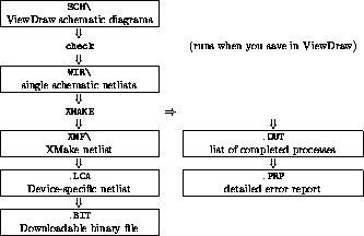
XMake compiles your schematic into a form that can be downloaded into a Xilinx FPGA. This process can take up to fifteen minutes for this lab. The flow is shown in Figure 1.
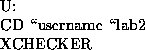
Start up the special DOS prompt for working with the Xilinx tools. You need to run the Xilinx tools from a special dos prompt, in the Xilinx program group. It is called NTXILINX.
Run ViewVsm manually on your design![]() .
This should report 0 errors and 0 warnings.
.
This should report 0 errors and 0 warnings.
Run XMake with XMAKE -P 4005PC84-6 FSM. The syntax is XMAKE -P part schematicName. The part number can be seen on the xilinx chip in the demoboard. If you ever have to deal with a different type of xilinx chip, you must rerun xmake.
If errors occur during XMake, check the .OUT and the .PRP![]() files. At least fifteen other files are also created, of varying
utility. The .RPT file is interesting if the XMake is
successful.
files. At least fifteen other files are also created, of varying
utility. The .RPT file is interesting if the XMake is
successful.
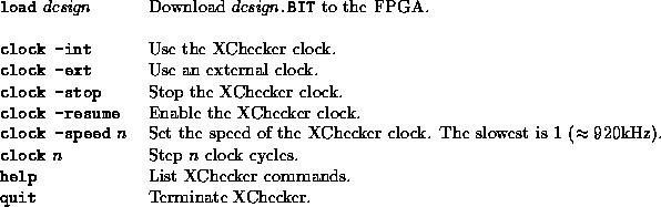
Table 1: Some XChecker commands.
XChecker is Xilinx's real-time hardware debugging tool, something like gdb for debugging hardware. The XChecker program communicates with the XC4003[A] through the XChecker cable. Table 1 lists some useful XChecker commands.
The power supplies have a cable with two banana plugs, red and black,
and a yellow lead. The black is ground, the red is +5V, and the
yellow is  V. Don't attach the V connector to anything,
and make sure it doesn't touch anything metal!
V. Don't attach the V connector to anything,
and make sure it doesn't touch anything metal!
Plug in the power supply.
Ground yourself.
Connect the black banana plug to the board.
Connect the red banana plug. The decimal point on CR3 should light, indicating the power is on.
Make sure Windows is not running.
Run XChecker at the NTXILINX prompt:
If this complains about the cable not being connected correctly, make sure the board has powered.
Make sure SW 4-7 (marked RST on the board) is closed. Otherwise, the RESET button won't work.
Type load FSM, and press Enter to confirm the load. XChecker will download FSM.BIT into the XC4005. A 0 should appear on CR4, indicating the machine is in State 0.
Test a successful combination using the buttons and switches on the
design demonstration board (see Figure ![]() for connections).
for connections).
Test an unsuccessful combination.
Have your TA check off your working lock.
Try stopping and restarting the clock:
Stop the clock with clock -stop. The decimal point on CR3 goes off and the lock stops working.
Restart the clock with clock -resume. The decimal point on CR3 illuminates and the lock works.
Name:Name:
Lab Section (Check one)
What is ENTER connected to (include direct and indirect sources)? Why?
What do you expect to see to see when the lock is opened?
To where does the clock feed out? Why?
Why are CODE0 and CODE1 not debounced?
In terms of buttons, switch settings, and lights illuminating, give instructions for opening the lock.
Explain the three wire-wrap wires on the board. Why are they there? Why does SW 4-7 have to be closed? (Hint: look at a board and the demonstration board schematics)
By looking at the report files, how many CLBs does your design use?
Working Xilinx Lock
Questions answered
Turned in on time: