-0V, marked
  ,
,  ,
and respectively. There is also a ground connection labeled
COM.
,
and respectively. There is also a ground connection labeled
COM.
Test Equipment
Building buggy hardware is easy, so you need some way to debug it. XChecker is a fantastic tool for debugging hardware, but it has limits and not everything has an XChecker cable connection.
This lab will familiarize you with more hardware debugging tools. Each station in 204B has a triple-output bench power supply, a digital multimeter, a 100 MHz digital storage oscilloscope, and a logic analyzer. You will use each of these in this lab.
Test equipment can be complex. The oscilloscope has more than fifty knobs and switches. Unfortunately, missetting these can make the equipment appear broken.
If you suspect faulty equipment, verify it with your TA! Don't take other stations' equipment.
When you leave the lab, please tidy up around your station. The TAs are not your mothers.
As usual, read through this lab. Most of this handout describes things to know, not things to do. And these should be easy if you know how to do them. Exercises start in Section 8.
War surplus plug-in power supplies![]() are not the only source of DC current.
Each station has an HP 6235A triple-output power supply, whose three
outputs can generate 0-6V, 0-18V, and -0V, marked , ,
and respectively. There is also a ground connection labeled
COM.
are not the only source of DC current.
Each station has an HP 6235A triple-output power supply, whose three
outputs can generate 0-6V, 0-18V, and -0V, marked , ,
and respectively. There is also a ground connection labeled
COM.
The HP's outputs are current-limited for safety: they will supply some maximum amount of current, and will drop the output voltage to ensure it. In particular, if you short the outputs, instead of blowing fuses or becoming arc welders, these supplies peacefully supply the maximum current.
The HP's three knobs set the voltage on the output, the voltage
on the output, and the ratio between the and
outputs.
The HP's analog meter can display the voltage or current for each
output, selected with the V A switch, and the three buttons
labeled , , and . This is useful for setting the
voltages approximately, but it is not as accurate as measuring the
output voltage with a digital multimeter.
Each station also has a Fluke 8010A digital multimeter, which can measure AC or DC voltage, current, resistance, or conductivity.
Connect the COMMON input (a black lead) to the circuit's
ground, and connect the V/k /S input (a red lead) to the
voltage to measure.
/S input (a red lead) to the
voltage to measure.
Connect the COMMON input and either the mA or the 10A max input in series with the wire whose current you wish to measure. This requires disconnecting the wire, often after the circuit is powered down.
With the circuit power off, connect the COMMON (black) and
V/k/S (red) leads across the resistive element. To do this
accurately, the element usually has to be removed from the circuit,
although simple continuity checking (determining if a wire is
connected) can be done in-circuit.
The pulse generator can generate single or periodic square waveforms with varying voltages, periods, duty cycles, pulse widths, and slew rates. These can be used, for example, as a digital system's clock.
The output of the pulse generator has a  output impedance,
and expects to be driving a load. Thus, with
high-impedance inputs such as those on digital logic or a scope, the
voltage you observe will be twice as large as what you set.
output impedance,
and expects to be driving a load. Thus, with
high-impedance inputs such as those on digital logic or a scope, the
voltage you observe will be twice as large as what you set.
To produce a square wave,
Make sure the DISABLE button (in the lower right corner) is off (unlit).
Set MODE to NORMAL by pressing the button beneath it.
Set CTRL to disabled (nothing lit).
Press the button underneath until PER lights, and set the period using the vernier buttons.
Press the button underneath until DTY lights, and set the duty cycle using the vernier buttons.
Or, set the pulse width ( ) by
pressing the button under WID. Adjust using the vernier
buttons.
) by
pressing the button under WID. Adjust using the vernier
buttons.
Press the button under HIL and set the high voltage using the vernier buttons.
Press the button under LOL and set the low voltage using the vernier buttons.
Oscilloscopes can display very high-speed periodic events. Think of them as things that graph voltage versus time.
Figure 1 shows an oscilloscope's major component: the cathode ray tube (CRT), similar to that in a television. A large voltage (our scope uses 14,000 V) is placed across anode and cathode, causing electrons to fly from the negatively-charged cathode, through a vacuum, and smash into the positively-charged anode, illuminating a spot on its phosphorus coating. This bright spot disappears quickly, so for an image to appear stable, it must be redrawn many times a second.
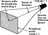
Figure 1: An Oscilloscope's Cathode Ray Tube (CRT)
To display a repeating waveform, the oscilloscope periodically ``sweeps'' the beam from left to right, vertically deflecting the beam proportional to the input voltage. The result is a graph with time increasing to the right, voltage increasing up: like a timing diagram.
Starting the sweep at the right time is necessary for a stable image. Figure 2a shows the effect of choosing the wrong times: many segments of the waveform are superimposed, resulting in an unreadable mess. If these times are chosen correctly, i.e., at some exact multiple of the period of the waveform, the traces superimpose to give a single, stable waveform, as shown in Figure 2b.
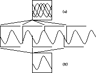
Figure 2: (a) Incorrect triggering. (b) Correct triggering.
Most oscilloscopes allow the user to set a voltage and a slope (rising or falling) for the trigger. For example, in Figure 2b, the trigger is the voltage halfway between the two extremes, with a falling slope. For simple waveforms, this by itself works well. For more complex waveforms, the variable holdoff control can help, which sets the time between the end of a sweep and when the scope starts looking for the trigger.
Not everything interesting is periodic; fortunately some oscilloscopes can record a single event and display it indefinitely. Once, such storage scopes used a clever electrical trick to keep the phosphors illuminated, but the advent of cheap, fast digital logic and memory made these obsolete.
DSOs, or digital storage oscilloscopes, digitize their inputs, store them in memory, and recall them through a digital-to-analog converter. Our Tektronix 2230s are DSOs.
Using a storage scope is much like using a non-storage scope: set the trigger to catch what you want and view the results. Instead of displaying the waveform for each trigger, however, a storage scope can await a single trigger, capture the waveform, and display it until you store another.
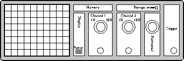
Figure 3: Groups of controls on
the 2230
The 2230 has some fifty knobs, buttons, and switches. Even for this lab, you need to know most of them. Fortunately, using one oscilloscope is like using another, so learning one is worth your time.
Here is a list of controls that concern you for this lab, grouped as in Figure 3:
THE TOPMOST CONCENTRIC KNOBS CONTROL THE BRIGHTNESS OF THE
NON-STORED WAVEFORMS. THE OUTER CONTROLS CHANNEL A: THE MAIN
DISPLAY.
IF NO WAVEFORMS APPEAR, SET THE CHANNEL A INTENSITY KNOB TO THE
MIDDLE.
JUST ABOVE THE FOCUS KNOB, THIS KNOB CONTROLS THE BRIGHTNESS
OF THE READOUT (VOLTS/DIVISION, SECONDS/DIVISION, THE TEK
LOGO) AND OF ALL STORED WAVEFORMS. TURNING THIS KNOB ALL THE WAY
COUNTERCLOCKWISE AND BACK TOGGLES WHETHER THESE ARE DISPLAYED AT
ALL.
IF STORED WAVEFORMS DO NOT APPEAR, TURN THIS KNOB FULLY
COUNTERCLOCKWISE AND BACK.
THE POWER SWITCH IS NEAR THE LOWER RIGHT CORNER OF THE DISPLAY (GRATICULE).
THIS TOPMOST KNOB MOVES THE WHOLE TRACE UP AND DOWN, EFFECTIVELY
SETTING THE ZERO POINT.
IF THE TRACE DOESN'T APPEAR, SET THIS KNOB TO POINT STRAIGHT
UP.
THE LEFTMOST LEVER, CH 1 BOTH CH 2, CHOOSES WHICH OF THE
CHANNELS IS DISPLAYED. THE X-Y AND BW LIMIT SWITCHES
SHOULD BE OUT. THE RIGHTMOST LEVER, ADD ALT CHOP, SELECTS HOW
TWO CHANNELS SHOULD BE DISPLAYED: USE ALT.
THE LARGE KNOB SETS THE NUMBER OF VOLTS PER VERTICAL DIVISION
DISPLAYED. FOR EXAMPLE, A 5V P-P SQUARE WAVE WILL BE DISPLAYED AS
ONE SQUARE HIGH IF THIS KNOB IS SET TO 5V/DIVISION.
READ THIS KNOB DIFFERENTLY DEPENDING ON THE PROBE. READ THE
THIS KNOB, IN THE CENTER OF THE LARGE ONE, IS A FINE ADJUSTMENT ON
THE NUMBER OF VOLTS/DIVISION. FOR NORMAL OPERATION, TURN IT ALL THE
WAY CLOCKWISE UNTIL IT CLICKS.
THIS LEVER, UNDER THE LARGE KNOB, SETS THE TYPE OF INPUT COUPLING
FOR THE CHANNEL. FOR NORMAL OPERATION, SET IT TO DC.
THIS TOPMOST KNOB MOVES BOTH TRACES LEFT AND RIGHT, EFFECTIVELY
SETTING WHERE THE TRIGGER POINT WILL APPEAR ON THE DISPLAY. SET
THIS TO POINT STRAIGHT UP.
SET THIS LEVER TO THE A POSITION.
THIS LARGE KNOB SETS HOW MANY SECONDS ARE DISPLAYED PER HORIZONTAL
DIVISION. THIS RANGES FROM HALF A SECOND TO AS LITTLE AS 50 NS.
THIS KNOB CAN PULL OUT FOR DELAYED-SWEEP MODE. LEAVE IT IN FOR
NORMAL OPERATION.
THIS SMALLER KNOB, IN THE CENTER OF THE SEC/DIV KNOB, IS A
FINE ADJUSTMENT ON THE NUMBER OF SECONDS PER DIVISION. FOR NORMAL
OPERATION, TURN IT ALL THE WAY CLOCKWISE UNTIL IT CLICKS.
THIS KNOB CAN BE PULLED OUT, MAGNIFYING THE TRACE TEN TIMES
HORIZONTALLY. LEAVE IT IN FOR NORMAL OPERATION.
THIS TOPMOST KNOB SETS THE AMOUNT OF TIME BETWEEN WHEN A SWEEP ENDS
AND WHEN THE TRIGGER STARTS LOOKING AGAIN. NORMALLY, THIS SHOULD BE
TURNED ALL THE WAY COUNTERCLOCKWISE.
THESE THREE BUTTONS SET THE SORT OF TRIGGERING. DEPRESS THE CENTER
ONE TO PUT THE SCOPE IN AUTOTRIGGERING MODE. HERE, THERE IS A
TIMEOUT ON THE TRIGGER, SO EVEN IN THERE IS NO INPUT, A TRACE WILL
STILL BE DISPLAYED.
WHEN THE OSCILLOSCOPE IS TRIGGERED, A LITTLE GREEN LED BELOW
THESE BUTTONS SHOULD LIGHT. IN P-P AUTO MODE, THIS SHOULD BE
CONSTANTLY LIT.
THIS SWITCH AND KNOB, JUST BELOW THE THREE TRIGGER SELECTION
BUTTONSTHERE IS ANOTHER PAIR, MARKED B TRIGGER, JUST
ABOVE. THESE ARE UNUSED IN THIS LAB., SET THE VOLTAGE AND THE
SLOPE OF THE INPUT FOR THE TRIGGER.
IN THE CENTER OF THE LEVEL KNOB IS ANOTHER KNOB, ACTUALLY A
SWITCH, LABELED HF REJECT. THIS SHOULD BE TURNED
COUNTERCLOCKWISE (TO OFF) FOR THIS LAB.
THESE TWO LEVERS, JUST ABOVE THE EXT INPUT BNC, SET THE
SOURCE OF THE MAIN TRIGGER. FOR THIS LAB, SET THE MIDDLE TO INT (USE THE INTERNAL TRIGGER SOURCE), AND THE LEFT TO CH 1
(EXAMINE CHANNEL 1 FOR THE TRIGGER). WE WON'T USE THE RIGHT LEVER.
THIS LEFTMOST SWITCH SHOULD BE IN (THE WAVEFORM REFERENCE
POSITION) FOR NORMAL SCOPE OPERATION.
THE LEFTMOST KNOB'S FUNCTION IS CONTROLLED BY THE SWITCH IMMEDIATELY
TO ITS RIGHT. WHEN THE SWITCH IS IN, THE KNOB MOVES ONE OF THE TWO
CURSORS ON THE STORED WAVEFORM; THE BUTTON IN THE CENTER OF THE KNOB
TOGGLES BETWEEN CURSORS. WHEN THE SWITCH IS OUT, THE KNOB SELECTS
WHICH STORED WAVEFORM IS DISPLAYED.
THIS SWITCH CONTROLS THE AMOUNT OF DATA STORED: ONE SCREEN IN THE 1K
MODE (IN), FOUR IN THE 4K MODE (OUT).
THIS SWITCH SETS WHEN DATA ACQUISITION WILL OCCUR RELATIVE TO THE
TRIGGER. IN THE POSTTRIG POSITION (OUT), SAMPLING WILL OCCUR
AFTER THE TRIGGER; IN THE PRETRIG POSITION (IN), SAMPLING WILL
OCCUR BEFORE THE TRIGGER.
IN STORAGE MODE, THE TRIGGER WILL APPEAR AS A T FLOATING ABOVE
THE TRACE.
WHEN THIS SWITCH IS OUT (CONTINUE), THE WAVEFORM BEING STORED
IS CONTINUALLY UPDATED. WHEN THIS SWITCH IS IN (SAVE), THE
STORED WAVEFORM IS HELD.
WHEN THIS SWITCH IS OUT (NON STORE), THE 2230 ACTS LIKE A
NORMAL SCOPE. WHEN THIS SWITCH IS IN (STORE), THE STORAGE
FEATURES ARE ENABLED.
Make sure the STORE button is out (NON STORE mode).
Connect the input to the Channel 1 BNC, set the coupling to
DC, set volts per division based on the amplitude of the
signal, make sure the CAL knob is fully clockwise, set the
leftmost Vertical Mode switch to CH 1, and adjust the
 POSITION knob to the center.
Set the A AND B SEC/DIV based on the period of the input, make
sure the CAL knob is fully clockwise, set the HORIZONTAL
MODE switch to A, and set the  POSITION
 knob to the center.
Make sure the P-P AUTO button is pressed, CH 1 is chosen for the internal trigger source, and A SOURCE is set to INT. Adjust the slope and trigger level to obtain a stable waveform.
Set the scope to display a periodic waveform, as explained above. Of particular importance are the volts per division and seconds per division settings
Make sure the STORE button is in (STORE mode).
While the SAVE/CONTINUE button is out, the scope is storing every input waveform. To save one, depress this button.
Although four-channel scopes exist, most digital circuits have far more than four interesting signals, and the ``interesting'' things on those signals are too complex for an oscilloscope's simple trigger to find. Logic analyzers address these problems.
Logic analyzers are like many-channeled storage oscilloscopes with very sophisticated schemes for triggering. Some logic analyzers have hundreds of channels, and the triggers can be little programs consisting of comparisons, loops, and branches. Logic analyzers capture and store digital waveforms only (i.e., usually only two voltage levels), and are typically not as fast as oscilloscopes. But for finding subtle, aperiodic bugs in digital hardware, they are unmatched.
The HP's power switch is on the top center of the rear panel. Upon
startup, it performs a self-test and loads some things from its
 floppy drive.
The controls of the HP are dominated by a single large knob, which is used for just about everything-something like a mouse. The select button in the upper-right corner chooses or changes what is highlighted by the knob.
Above the keypad are four MENU buttons labeled FORMAT, TRACE, DISPLAY, and I/O. These each bring up one of the four main menus:
HERE, YOU GROUP AND NAME SETS OF INPUT BITS. A SUBMENU ALLOWS YOU TO NAME A GROUP'S BIT PATTERNS.
HERE, YOU SPECIFY THE TRIGGER CONDITION(S).
HERE, THE CAPTURED BIT PATTERNS ARE DISPLAYED.
THE MARKERS POP-UP LETS YOU ENABLE AND DISABLE CURSORS, WHICH CAN BE PLACED AT ARBITRARY POINTS IN THE STORED DATA TO MEASURE TIME DELAYS.
THE ACCUMULATE FLAG, WHEN SET, MAKES ADDITIONAL GATHERED DATA DRAW OVER THE EXISTING DATA.
THE TIME/DIV SETTING CONTROLS HOW MUCH THE DISPLAY IS ZOOMED HORIZONTALLY.
THE DELAY SETTING CONTROLS WHAT IS DISPLAYED IN THE CENTER OF THE WINDOW, RELATIVE TO THE TRIGGER.
THIS GIVE ACCESS TO THE DISK, AND STARTS A SELF-TEST. YOU PROBABLY WON'T HAVE NEED OF THESE FACILITIES.
TO START CAPTURING, PRESS THE RUN BUTTON (TO THE LEFT OF THE KEYPAD). THIS WILL AWAIT THE TRIGGER AND FILL THE MEMORY. IF A TRIGGER EVENT IS TOO LONG IN COMING, PRESS STOP TO ABORT.
WHEN THE SYSTEM FIRST STARTS, OR IF YOU CHOOSE SYSTEM IN THE UPPER LEFT CORNER OF ANY MENU, THE SYSTEM CONFIGURATION MENU APPEARS. THE BIG SETTING HERE IS ``TYPE,'' WHICH LETS YOU CHOOSE BETWEEN TIMING MODE, WHERE THE DISPLAY IS TIMING-DIAGRAM BASED, AND STATE, WHERE THE DISPLAY IS MORE LIKE A TRUTH TABLE.
Use banana leads to connect the output of the power supply to the input of the multimeter. Use black for common, red for power.
Adjust the supply to simultaneously generate  V,
V,  V, and
 V, and measure this with the multimeter. Show your TA this.
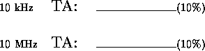
Connect the output of the HP 8112A Pulse Generator to Channel 1 of the scope using a coaxial cable with BNC ends.
Set the pulse generator to generate a 10 kHz, 45% duty cycle, 4
volt peak-to-peak, zero volt offset (i.e., peaks at  V) square
wave.
V) square
wave.
Display this square wave using the NON STORE and STORE modes of the scope. In the STORE mode, use the cursors to verify the times and voltages. Show your TA this.
Set the pulse generator to generate a 10 MHz, 0-5V square wave with a 40 ns pulse width.
Again, display this with both modes of the scope, verifying times and voltages in the STORE mode. Show your TA this.
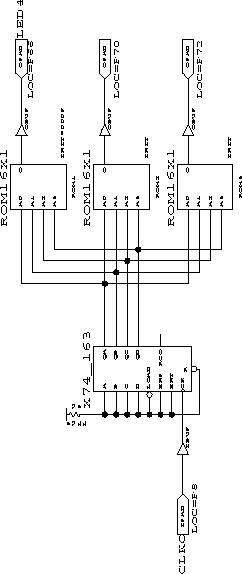
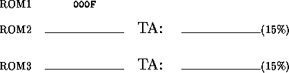
We have entered and compiled the circuit in Figure 4, a four-bit counter driving the addresses of three sixteen-bit ROMs. Your task will be to use both channels of the oscilloscope to observe the outputs of ROM2 and ROM3 and deduce their contents, using the contents of ROM1 as a starting point.
The counter counts 0000, 0001, ..., 1111, and repeats.. Address 0000 reads the least significant bit of the four-digit hex number in the ROM, address 1111 the most. So if one of the ROMs contained ones in addresses 0001 through 1111, and a zero in address 0000, the ROM contents would be FFFE. See the ROM16X1 page in your reader for more information.
Fire up XChecker and load the ROM circuit: U:'134 WVLIB'134 CS150'134 '134 ROM.BIT. If all goes well, the fourth LED will light (the output of ROM1).
Connect the BNC ends of the scope probes to the scope's
Channel 1 and Channel 2 inputs. These are  probes, so the
volts/div reading on the scope's display will be a tenth of the
circuit's voltages.
probes, so the
volts/div reading on the scope's display will be a tenth of the
circuit's voltages.
Carefully connect each probe's ``hook'' to one of the wire-wrap pins connected to a Xilinx pin connected to a ROM's output. Be careful not to short together two pins, and don't let the probe bend the pin. Connect Channel 1 to the output of ROM1, whose contents you know, and connect Channel 2 to the output of one of the others.
Connect both probes' alligator clips to a ground reference in the prototyping area of the board.
Set the oscilloscope to trigger on Channel 1 (the output of ROM1), and display both channels.
Adjust the CAL knob in the center of the SEC/DIV knob to make exactly two bits display per division-adjust it so eight divisions occur between rising edges in the output of ROM1.
Read off the bits from each ROM, moving the Channel 2 probe between pins to view the contents of the two ROMs, and translate each into a four-digit hex number. Record these on the checkoff sheet and show your TA.
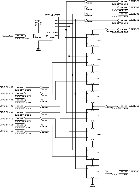
We have entered and compiled the circuit in Figure 5, a eight-bit ripple adder summing the output of a four-bit counter and four switches. Your task will be to measure the worst-case delay of the circuit.
The worst-case delay occurs when a carry must ripple through each stage, such as when 1111 and 0001 are added. To find this, set the switches to 0001, and set the logic analyzer to trigger when the counter hits 1111.
Fire up XChecker and load the adder: S U:'134 WVLIB'134 CS150'134 ADD.BIT. If all goes well, you should see the left four LEDs light.
Since the outputs all go to LEDs, this circuit is an excellent one to single-step with the clock. Stop the clock and use the CLOCK command to step the counter. The adder will still work even when the clock is stopped. Remember that the LEDs light when their output is low.
Connect the logic analyzer's pod's black ground lead to a ground reference (e.g., one of the ground pins on the Xilinx), and connect seven of the eight inputs to the four counter outputs and three adder outputs.
Be careful when connecting the probe leads. They are delicate and expensive, even more so than the wire-wrap posts.
Set the switches so 00000001 is one of the addends.
Set the trigger on the logic analyzer to when the counter reaches 1111.
Measure the delay from when the counter output changes to when the final carry-out changes, and record this on the checkoff sheet. Show your TA this.
Name:Name:
Lab Section (Check one)
Power Supply and Multimeter
Pulse Generator and Oscilloscope
ROMs
Logic Analyzer Delay: