Project 3 CPU Design in Logisim
Project 3-1: ALU and RegFile
Deadline: Sunday, March 10th, 2019 at 11:59pm
Getting Started
Starter Files and Setup
Please accept the Github Classroom assignment by clicking this link. Once you’ve created your repository, you’ll need to clone it to your instructional account and/or your local machine. You’ll also need to add the starter code remote with the following command:
git remote add staff https://github.com/61c-teach/sp19-proj3-starter
If we publish changes to the starter code, retrieve them using git pull staff master. Any updates will be recorded in the Clarifications and Updates section below, so check there to see if there are any changes for you to pull.
Files for Project 3-1 can be found in the part1 directory; Project 3-2 will be released shortly, at which time you’ll see files in a part2 directory.
As in Lab 6, you will be working on this project in Logisim Evolution. It is our recommendation that you work on your circuits with Logisim locally. You can run Logisim Evolution with the following command:
java -jar logisim-evolution.jar
Logisim Evolution is a Java program; if you get an error along the lines of java: command not found when you try to run the command above, you likely need to install Java. Head over to this page on the CS 61B website for instructions on installing Java for Windows, Mac, and Linux.
The testing scripts require Python; if you don’t have Python installed on your local machine, head over to this page on the CS 61A website for instructions on installing Python for Windows, Mac, and Linux.
You can also run Logisim Evolution over SSH. This should ideally be your second choice, after trying to use it locally. If you want to run a graphical program over SSH, you should use the -XY flag, e.g.
ssh -XY cs61c-xxx@hiveYY.cs.berkeley.edu
If you get an error doing this, some suggestions: if you’re on Mac, download XQuartz, and try the above again.
If you’re on Windows, download MobaXterm, and use that as your terminal when SSH-ing to run Logisim.
Please read the entire spec before beginning the project.
General Advice
Save frequently and commit frequently! Try to save your code in Logisim every 5 minutes or so, and commit every time you produce a new feature, even if it is small.
Tests for a completed ALU and RegFile have been included with the lab starter code. You can run them with the command ./test.sh. See the Testing section for information on how to interpret your test output. The final submission for the project will be through Gradescope, but the tests will be exactly the same as those that are run with test.sh.
Don’t move around the given inputs and outputs in your circuit; this could lead to issues with the autograder.
Because the files you are working on are actually XML files, they’re quite difficult to merge properly. We strongly recommend against working on your files in two separate places and attempting to merge later; you may lose valuable work.
Clarifications and Updates
Any clarifications and/or updates about this project will be posted both here and on the Project 3-1 Index Post on Piazza. The Piazza post will also have a small selection of particularly useful/insightful followups at the top that you might find useful to read through if you get stuck.
Resources
The lectures that covered the material relevant to this project were Lecture 11 on Thursday February 28th (RISC-V Datapath, Single-Cycle Control Intro) and Tuesday March 5th (RISC-V Single-Cycle Control). The relevant reading from Patterson & Hennessey is Chapter 4.1 - 4.4.
Exercise 1: Arithmetic Logic Unit (ALU)
Your first task is to create an ALU that supports all the operations needed by the instructions in our ISA (which is described in further detail in the next section). Please note that we treat overflow as RISC-V does with unsigned instructions, meaning that we ignore overflow.
We have provided a skeleton of an ALU for you in alu.circ. It has three inputs:
| INPUT NAME | BIT WIDTH | DESCRIPTION |
| A | 32 | Data to use for Input A in the ALU operation. |
| B | 32 | Data to use for Input B in the ALU operation. |
| ALUSel | 4 | Selects what operation the ALU should perform (see the list of operations with corresponding switch values below). |
… and one output:
| OUTPUT NAME | BIT WIDTH | DESCRIPTION |
| Result | 32 | Result of the ALU Operation. |
Below is the list of ALU operations for you to implement, along with their associated ALUSel values. All of them are required with the exception of mulh, which will take some extra effort to implement (but you’re certainly up to the task!) You are allowed and highly encouraged to use built-in Logisim blocks to implement the arithmetic operations.
| Switch Value | Instruction |
| 0 | add: Result = A + B |
| 1 | and: Result = A & B |
| 2 | or: Result = A | B |
| 3 | xor: Result = A^B |
| 4 | srl: Result = (unsigned) A >> B |
| 5 | sra: Result = (signed) A >> B |
| 6 | sll: Result = A << B |
| 7 | slt: Result = (A < B) ? 1 : 0 Signed |
| 8 | divu: Result = (unsigned) A / B |
| 9 | remu: Result = (unsigned) A % B |
| 10 | mult: Result = (signed) A*B[31:0] |
| 14 | mulh: Result = (signed) A*B[63:32] |
| 11 | mulhu: Result = A*B[63:32] |
| 12 | sub : Result = A - B |
| 13 | bsel: Result = B |
When implementing mul, mulh, and mulhu, notice that the multiply block has a “Carry Out” output, located here:
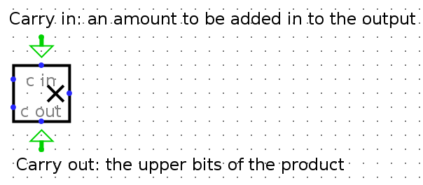
Experiment a bit with it, and see what you get for both the result and carryout with negative and positive 2’s complement numbers. You should realize why we made mulh extra credit.
Hints
Add is already made for you, and feel free to use a similar structure when implementing your other blocks.
You can hover your cursor over an output/input on a block to get more detailed information about that input/output.
You might find bit splitters or extenders useful when implementing sra and srl.
Use tunnels! They will make your wiring cleaner and easier to follow, and will reduce your chances of encountering unexpected errors.
- A multiplexer (MUX) might be useful when deciding which block output you want to ouput. In other words, consider simply processing the input in all blocks, and then outputing the one of your choice.
As long as you don’t move the input/output pins or change the shape of the circuit, you can make any modifications to alu.circ you want so that the outputs must obey the behavior specified above. Your alu.circ that you submit must fit into the alu_harness.circ file we have provided for you. To verify changes you have made didn’t break anything, you can open alu_harness.circ or any of the .circ files in the test directory and ensure there are no errors and that the circuit functions well. (The tests use a slightly modified copy of alu_harness.circ.)
Exercise 2: Register File (RegFile)
As you learned in class, RISC-V architecture has 32 registers. However, in this project, You will only need implement 9 of them (specified below) to save you some repetitive work. This means your rs1, rs2, and rd signals will still be 5-bit, but we will only test you on the specified registers. You will not be docked points in any way for implementing all 32 registers. These are the 9 we will test.
Your RegFile should be able to write to or read from these registers specified in a given RISC-V instruction without affecting any other registers. There is one notable exception: your RegFile should NOT write to x0, even if an instruction tries. Remember that the zero register should ALWAYS have the value 0x0.
You should NOT gate the clock at any point in your RegFile: the clock signal should ALWAYS connect directly to the clock input of the registers without passing through ANY combinational logic.
The registers and their corresponding numbers are listed below.
| Register # | Register Name |
| x0 | zero |
| x1 | ra |
| x2 | sp |
| x5 | t0 |
| x6 | t1 |
| x7 | t2 |
| x8 | s0 |
| x9 | s1 |
| x10 | a0 |
You are provided with the skeleton of a register file in regfile.circ. The register file circuit has six inputs:
| Input Name | Bit Width | Description |
| Clock | 1 | Input providing the clock. This signal can be sent into subcircuits or attached directly to the clock inputs of memory units in Logisim, but should not otherwise be gated (i.e., do not invert it, do not "and" it with anything, etc.). |
| RegWEn | 1 | Determines whether data is written to the register file on the next rising edge of the clock. |
| Read Register 1 (rs1) | 5 | Determines which register's value is sent to the Read Data 1 output, see below. |
| Read Register 2 (rs2) | 5 | Determines which register's value is sent to the Read Data 2 output, see below. |
| Write Register (rd) | 5 | Determines which register to set to the value of Write Data on the next rising edge of the clock, assuming that RegWEn is a 1. |
| Write Data | 32 | Determines what data to write to the register identified by the Write Register input on the next rising edge of the clock, assuming that RegWEn is 1. |
The register file also has the following outputs:
| Output Name | Bit Width | Description |
| Read Data 1 | 32 | Driven with the value of the register identified by the Read Register 1 input. |
| Read Data 2 | 32 | Driven with the value of the register identified by the Read Register 2 input. |
| ra Value | 32 | Always driven with the value of `ra` (This is a DEBUG/TEST output.) |
| sp Value | 32 | Always driven with the value of `sp` (This is a DEBUG/TEST output.) |
| t0 Value | 32 | Always driven with the value of `t0` (This is a DEBUG/TEST output.) |
| t1 Value | 32 | Always driven with the value of `t1` (This is a DEBUG/TEST output.) |
| t2 Value | 32 | Always driven with the value of `t2` (This is a DEBUG/TEST output.) |
| s0 Value | 32 | Always driven with the value of `s0` (This is a DEBUG/TEST output.) |
| s1 Value | 32 | Always driven with the value of `s1` (This is a DEBUG/TEST output.) |
| a0 Value | 32 | Always driven with the value of `a0` (This is a DEBUG/TEST output.) |
The DEBUG/TEST outputs are present for testing and debugging purposes. If you were implementing a real register file, you would omit those outputs. In our case, be sure they are included correctly–if they are not, you will not pass.
As long as you don’t move the input/output pins or change the shape of the circuit, you can make any modifications to regfile.circ you want so that the outputs must obey the behavior specified above. Your regfilecirc that you submit must fit into the regfile_harness.circ file we have provided for you. To verify changes you have made didn’t break anything, you can open regfile_harness.circ or any of the .circ files in the test directory and ensure there are no errors and that the circuit functions well. (The tests use a slightly modified copy of regfile_harness.circ.)
Hints
Take advantage of copy-paste! It might be a good idea to make one register completely and use it as a template for the others to avoid repetitive work.
Because of the naming conventions that Logisim Evolution requires, because the outputs are named ra, sp, etc., you will not be able to name your registers ra, sp, etc. We suggest that you instead name them with numerical name of the register, e.g. x1, x2.
It is inadvisable to use the enable input on your MUXes. In fact, you can turn that feature off. We’d also recommend that you turn “three-state?” to off.
MUXes are your friend, but don’t forget about DeMUXes.
Think about what happens in the register file after a single instruction is executed. Which values change? Which values stay the same? Registers are rising-edge triggered–what does that mean?
Keep in mind registers have an “enable” input available, as well as a clock input.
Testing
We test your Logisim circuits using “harness” files that feed our test data as input into your circuits and have output pins connected to each of the outputs of your circuits. When Logisim is run from the command line, it outputs the values in each of the input/output pins at each clock tick.
When you run ./test.sh, the ALU and RegFile tests will produce output in the tests/student_output directory. These outputs will be difficult to interpret 0’s, 1’s, and possibly x’s, if your circuit produces any undefined output. We’ve provided two python scripts called binary_to_hex_alu.py and binary_to_hex_regfile.py that can interpret this output in a readable format for you. To use them, do the following: (you may have to use “py” or “python3” as is appropriate on your machine)
cd tests
python binary_to_hex_alu.py PATH_TO_OUT_FILE
For example, to see reference_output/alu-add-ref.out in readable format, you would do this:
cd tests
python binary_to_hex_alu.py reference_output/alu-add-ref.out
If you want to see the difference between your output and the reference solution, put the readable outputs into new .out files and diff them. For example, for the alu-add test, take the following steps:
cd tests
python binary_to_hex_alu.py reference_output/alu-add-ref.out > alu-add-ref.out
python binary_to_hex_alu.py student_output/alu-add-student.out > alu-add-student.out
diff alu-add-ref.out alu-add-student.out
If you get error: permission denied when attempting to run test.sh, you may need to use chmod to set the appropriate permissions, as follows (from your proj3/part1 directory):
chmod +x tests/test.py test.sh
Submission
Your final submission for this project will be on Gradescope. It is available now! The name of the assignment is “Project 3-1: ALU and RegFile”. Please upload your alu.circ and regfile.circ files. The autograder should not take more than 3 minutes to run.
Project 3-2: 2-stage Pipelined RISC-V Datapath
Deadline: Saturday March 23rd, 2019 at 11:59pm
Overview
In the second part of this project, you will be using logisim-evolution to implement a 32-bit two-cycle processor based on RISC-V. Once you’ve completed this project, you’ll know essentially everything you need to build a computer from scratch with nothing but transistors. Hopefully this project will bring you your hand-of-software touches hand-of-hardware moment!

There are a lot of parts to this spec, but we really do recommend you read over everything before starting! Be sure to reference the Getting Started Guide for a place to begin–it guides you through each stage of the processor and will help you pass the first sanity test.
Starter Files and Setup
We’ve added the Project 3-2 files to the starter code repository; you can get them in two steps.
First, add the starter as a remote repository:
git remote add starter https://github.com/61c-teach/sp19-proj3-starter.git
Second, pull the starter files using this command:
git pull starter master
We will provide you with skeleton code that includes sanity tests along with a CPU template (cpu.circ), harness (run.circ), and the data memory module (mem.circ). The shell script to run the sanity tests and to run the tests you’ve created yourself copies your alu.circ and regfile.circ into the appropriate directory from part1, so you won’t need to move anything.
We have hopefully prevented this, but if you get any sort of error: permission denied error, try the following from your part2 directory
chmod +x cpu-sanity.sh cpu-user.sh my_tests/circ_files/modular_test.py tests/circ_files/sanity_test.py
Clarifications and Updates
Any clarifications and/or updates about this project will be posted both here and on the Project 3-2 Index Post on Piazza. The Piazza post will also have a small selection of particularly useful/insightful followups at the top that you might find useful to read through if you get stuck.
Monday March 11 (10AM): If you pulled the starter code before 10:00AM on 3/11, re-pull! We fixed the starter code bug noted in the first followup below. If you have a merge conflict (you should only run into this if you already started working on the project), feel free to make a private post on Piazza and we’ll help you resolve it.
Resources
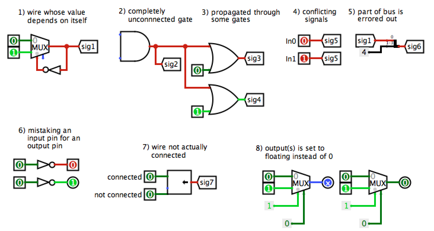
What do the different wire colors mean
Some common causes of errors in Logisim:
Instructions
(1) Processor
We have provided a skeleton for your processor in cpu.circ. You will be using your own implementations of the ALU and RegFile as you construct your datapath. If you find any errors in either of these components, you should definitely fix them, as you will want them working properly in order to run all of the tests, but you can choose whether or not you’d like your final implementation to use the staff solution ALU/RegFile or your own.
We have provided implementations of IMEM (the memory unit in run.circ) and DMEM (in cpu.circ), but otherwise, you are responsible for constructing the entire datapath and control from scratch. Your completed processor should implement the ISA detailed below in the section Instruction Set Architecture (ISA) using a two-cycle pipeline, with IF (instruction fetch) in the first stage and ID (instruction decode), EX (execute), MEM (memory), and WB (writeback) in the second stage, which collectively we call EX.
Your processor will get its program from the processor harness run.circ. Your processor will output the address of an instruction, and accept the instruction at that address as an input. Inspect run.circ to see exactly what’s going on. (Every test is simply a copy of this same harness.) Your processor has 2 inputs that come from the harness:
| Input Name | Bit Width | Description |
| INSTRUCTION | 32 | Driven with the instruction at the instruction memory address identified by the FETCH_ADDRESS (see below). |
| CLOCK | 1 | The input for the clock. As with the register file, this can be sent into subcircuits (e.g. the CLK input for your register file) or attached directly to the clock inputs of memory units in Logisim, but should not otherwise be gated (i.e., do not invert it, do not *AND* it with anything, etc.). |
and your processor must provide the following outputs to the harness:
| Output Name | Bit Width | Description |
| ra | 32 | Driven with the contents of ra. FOR TESTING |
| sp | 32 | Driven with the contents of sp. FOR TESTING |
| t0 | 32 | Driven with the contents of t0. FOR TESTING |
| t1 | 32 | Driven with the contents of t1. FOR TESTING |
| t2 | 32 | Driven with the contents of t2. FOR TESTING |
| s0 | 32 | Driven with the contents of s0. FOR TESTING |
| s1 | 32 | Driven with the contents of s1. FOR TESTING |
| a0 | 32 | Driven with the contents of a0. FOR TESTING |
| FETCH_ADDRESS | 32 | This output is used to select which instruction is presented to the processor on the INSTRUCTION input. |
Just like with the ALU and RegFile, be very careful NOT to move the input or output pins, and not to add any new input/output pins.
RISC-V assumes byte addressing (every 1 byte has a unique memory address), but the memory units we use in Logisim are word addressed (4 bytes/1 word share a single memory address). To account for this, in the skeleton code, we shift your program counter to the right by two bits for you, to convert it from a byte address to a word address; this word address is outputted from your CPU as FETCH_ADDRESS.
(1.5) Memory
The memory unit is already fully implemented for you! Here’s a quick summary of its inputs and outputs:
| Output Name | In- or Out-put | Bit Width | Description |
| A: ADDR | In | 32 | Address to read/write to in Memory |
| D: WRITE DATA | In | 32 | Value to be written to Memory |
| En: WRITE ENABLE | In | 1 | Equal to one on any instructions that write to memory, and zero otherwise |
| Clock | In | 1 | Driven by the clock input to `cpu.circ` |
| D: READ DATA | Out | 32 | Driven by the data stored at the specified address. |
You will pass a byte address into the memory unit, which will drop the last two bits of the address you pass in, as the memory we use in Logisim is word addressed. The memory unit always returns 4 bytes/1 word. Feel free to inspect mem.circ to see how this works. Do not make any changes to mem.circ, as we will use the version included with the starter code to test your final CPU. Feel free to move it within the skeleton, however.
(2) The Instruction Set Architecture
Your CPU will support the RISC-V instructions listed below, along with three custom instructions, lwc (load word conditional), push (push a value to the stack and decrement sp), and pop (pop some number of bytes off of the stack and increment the stack pointer). Besides these three instructions, all instructions should behave the same as the RISC-V you learned in class. These are not all of the instructions on the green card, but these are the only instructions you will be tested on implementing. You will not be punished for implementing other instructions (the autograder will cover ONLY the instructions below). If anything below surprises you, or seems to be in conflict with the green card/ISA manual, it is certainly possible that we made a mistake. Please make a Piazza post about it.
Instruction Formats
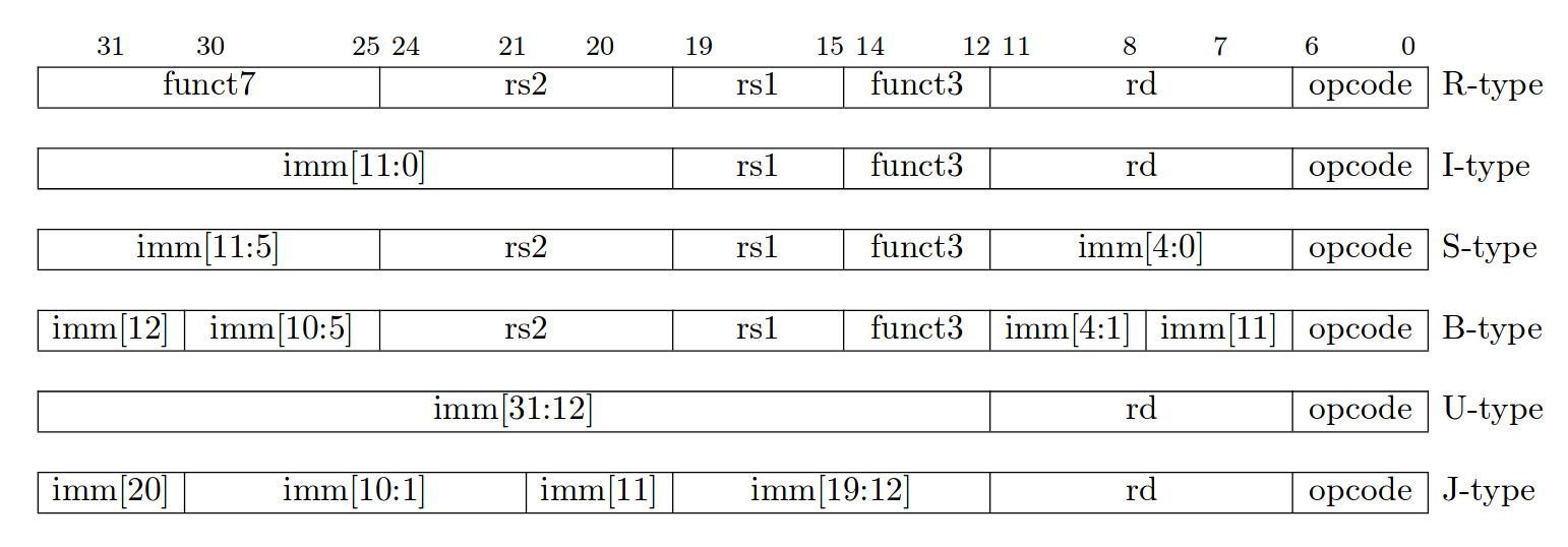
RISC-V Instructions
| Instruction | Type | Opcode | Funct3 | Funct7/IMM | Operation |
| add rd, rs1, rs2 | R | 0x33 | 0x0 | 0x00 | R[rd] ← R[rs1] + R[rs2] |
| mul rd, rs1, rs2 | 0x0 | 0x01 | R[rd] ← (R[rs1] * R[rs2])[31:0] | ||
| sub rd, rs1, rs2 | 0x0 | 0x20 | R[rd] ← R[rs1] - R[rs2] | ||
| sll rd, rs1, rs2 | 0x1 | 0x00 | R[rd] ← R[rs1] << R[rs2] | ||
| mulh rd, rs1, rs2 | 0x1 | 0x01 | R[rd] ← (R[rs1] * R [rs2])[63:32] | ||
| mulhu rd, rs1, rs2 | 0x3 | 0x01 | (unsigned) R[rd] ← (R[rs1] * R[rs2])[63:32] | ||
| slt rd, rs1, rs2 | 0x2 | 0x00 | R[rd] ← (R[rs1] < R[rs2]) ? 1 : 0 (signed) | ||
| xor rd, rs1, rs2 | 0x4 | 0x00 | R[rd] ← R[rs1] ^ R[rs2] | ||
| divu rd, rs1, rs2 | 0x5 | 0x01 | (unsigned) R[rd] ← R[rs1] / R[rs2] | ||
| srl rd, rs1, rs2 | 0x5 | 0x00 | R[rd] ← R[rs1] >> R[rs2] | ||
| sra rd, rs1, rs2 | 0x5 | 0x20 | R[rd] ← R[rs1] >> R[rs2] | ||
| or rd, rs1, rs2 | 0x6 | 0x00 | R[rd] ← R[rs1] | R[rs2] | ||
| remu rd, rs1, rs2 | 0x7 | 0x01 | (unsigned) R[rd] ← R[rs1] % R[rs2] | ||
| and rd, rs1, rs2 | 0x7 | 0x00 | R[rd] ← R[rs1] & R[rs2] | ||
| lb rd, offset(rs1) | I | 0x03 | 0x0 | -- | R[rd] ← SignExt(Mem(R[rs1] + offset, byte)) |
| lh rd, offset(rs1) | 0x1 | -- | R[rd] ← SignExt(Mem(R[rs1] + offset, half)) | ||
| lw rd, offset(rs1) | 0x2 | -- | R[rd] ← Mem(R[rs1] + offset, word) | ||
| addi rd, rs1, imm | 0x13 | 0x0 | -- | R[rd] ← R[rs1] + imm | |
| slli rd, rs1, imm | 0x1 | 0x00 | R[rd] ← R[rs1] << imm | ||
| slti rd, rs1, imm | 0x2 | -- | R[rd] ← (R[rs1] < imm) ? 1 : 0 | ||
| xori rd, rs1, imm | 0x4 | -- | R[rd] ← R[rs1] ^ imm | ||
| srli rd, rs1, imm | 0x5 | 0x00 | R[rd] ← R[rs1] >> imm | ||
| srai rd, rs1, imm | 0x5 | 0x20 | R[rd] ← R[rs1] >> imm | ||
| ori rd, rs1, imm | 0x6 | -- | R[rd] ← R[rs1] | imm | ||
| andi rd, rs1, imm | 0x7 | -- | R[rd] ← R[rs1] & imm | ||
| sw rs2, offset(rs1) | S | 0x23 | 0x2 | -- | Mem(R[rs1] + offset) ← R[rs2] |
| beq rs1, rs2, offset | SB | 0x63 | 0x0 | -- |
if(R[rs1] == R[rs2])
PC ← PC + {offset, 1b0} |
| blt rs1, rs2, offset | 0x4 | -- |
if(R[rs1] less than R[rs2] (signed))
PC ← PC + {offset, 1b0} |
||
| bltu rs1, rs2, offset | 0x6 | -- |
if(R[rs1] less than R[rs2] (unsigned))
PC ← PC + {offset, 1b0} |
||
| bne rs1, rs2, offset | 0x1 | -- |
if(R[rs1] != R[rs2])
PC ← PC + {offset, 1b0} |
||
| lui rd, offset | U | 0x37 | -- | -- | R[rd] ← {offset, 12b0} |
| jal rd, imm | UJ | 0x6f | -- | -- |
R[rd] ← PC + 4
PC ← PC + {imm, 1b0} |
| jalr rd, rs, imm | I | 0x67 | 0x0 | -- |
R[rd] ← PC + 4
PC ← R[rs] + {imm} |
Additional Instructions
lwc: Opcode=0b0000011, funct3=0b111
Format: lwc rd, imm(rs1), rs2 where imm == func7. lwc should look like an R-type instruction in the layout of its bits, even though its opcode is for loads (which are I-type instructions). Alternatively, you can think of lwc as an I-type where there is a constraint on the immediate field.
Operation:
if (R[rs2]) {
    R[rd] := M[R[rs1] + func7]
}
push: Opcode=0b0111011, funct3=0b011
Format: push rs2. push will also be an R-type instruction; the bits of the instruction in all fields that are unused (funct7, rs1) should be disregarded; you can assume they will be 0’s, which is what Venus will put there.
Operation:
R[sp] := R[sp] - 4

M[R[sp]] := R[rs2]
pop: Opcode=0b0111011, funct3=0b010
Format: pop imm. pop will be an I-type instruction, where imm is an I-type imm. The bits of the instruction in all fields that are unused (rs1, rs2) should be disregarded, as they serve no function; you can assume they will be 0’s, which is what Venus will put there.
Operation:
R[sp] := R[sp] + imm
Immediates:
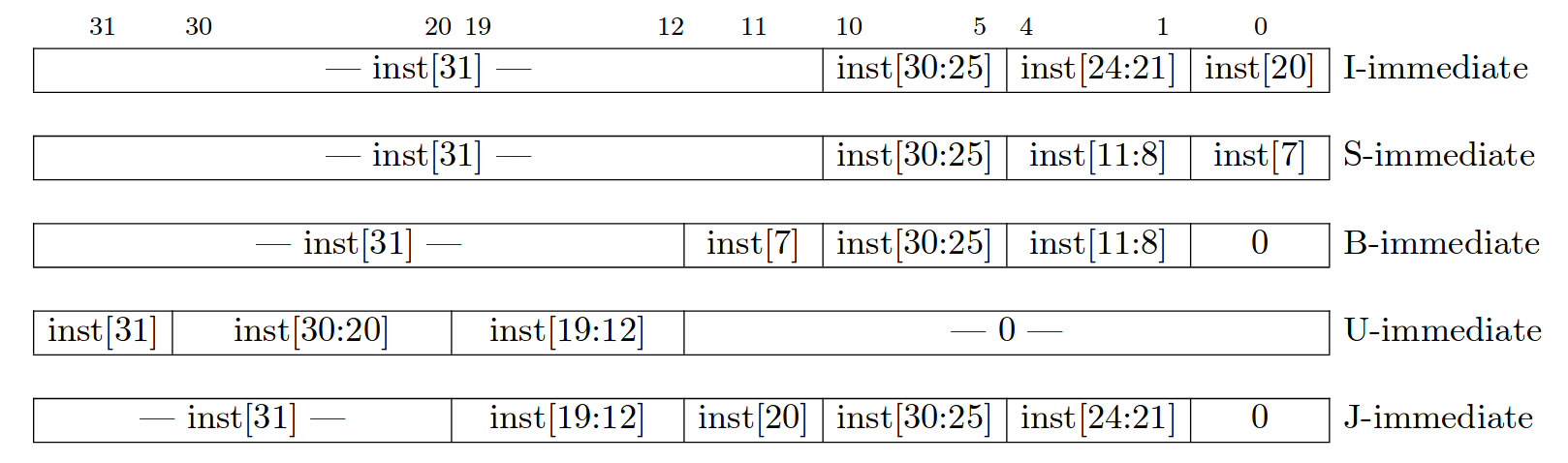
For I, S, B, U, and J type instructions, you will have to extract the appropriate immediate from the instruction. You may want to create an Immediate Generator subcircuit to do this. Remember that in RISC-V, all immediates that leave the immediate generator are 32-bits and sign-extended! You may find the following diagram helpful for thinking about how to create the appropriate immediate for each type:
(3) Controls
You can probably guess that control signals will play a very large part in this project. Figuring out all of the control signals may seem intimidating. We suggest taking a look at Discussion 6 to get started, and to remember that there is not a definitive set of control signals–walk through the datapath with different types of instructions, and when you see a mux or other component think about what selector/enable value you will need for that instruction. We suggest you create a “Control Module” subcircuit that takes in an instruction and outputs the control signals for that instruction.
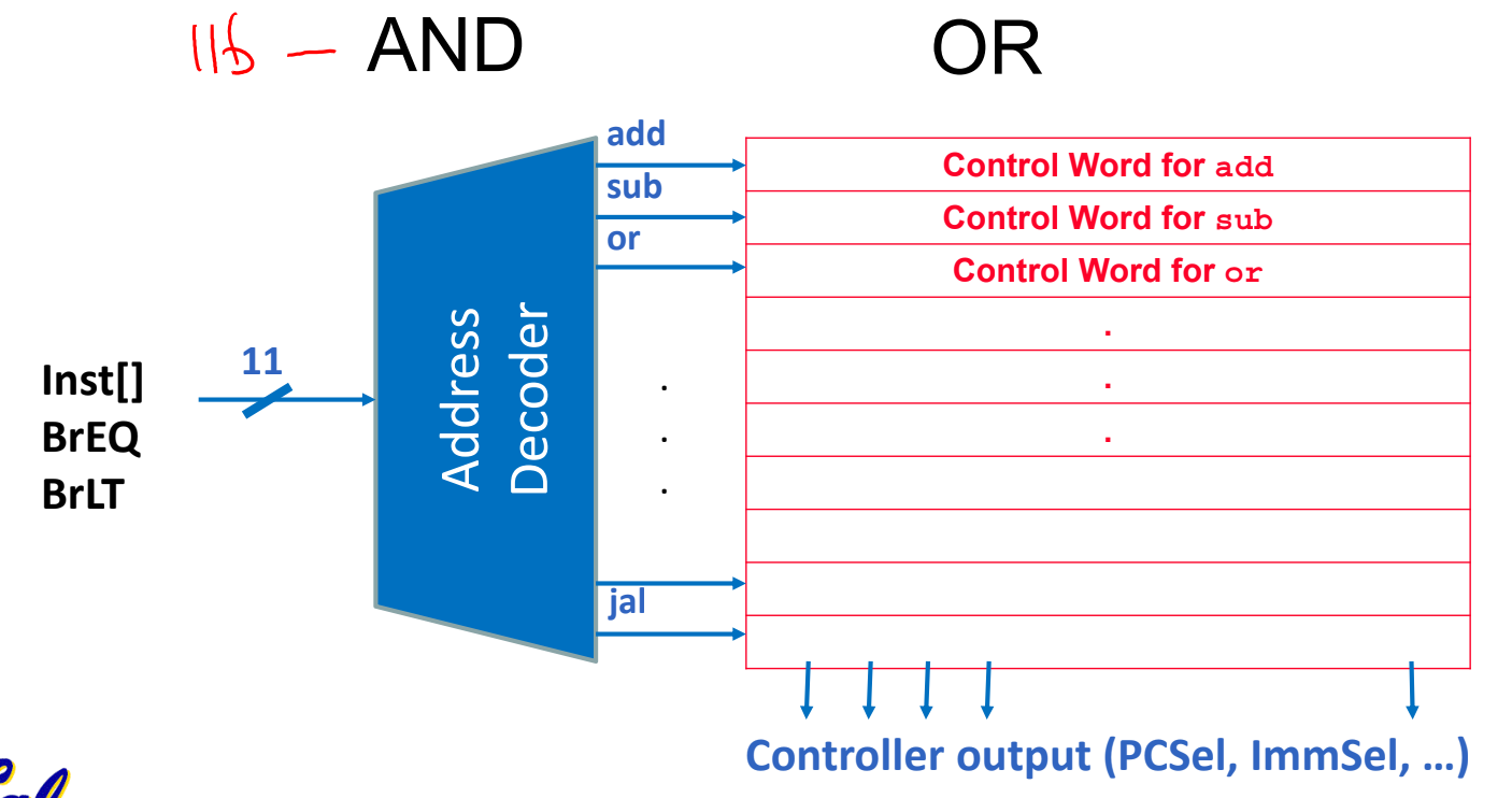
There are a two major approaches to implementing the Control so that it can translate the opcode/funct3/funct7 to the corresponding instruction and then set the control signals. One way to do, ROM control was outlined in lecture. Every instruction implemented by a processor maps to an address in a ROM (read-only memory) unit. At that address in the ROM is the control word for that instruction. An address decoder takes in an instruction and outputs the address of the control word for that instruction. This approach is common in CISC architectures like Intel’s x86-64, and offers some flexibility because it can be re-programmed by changing the contents of the ROM.
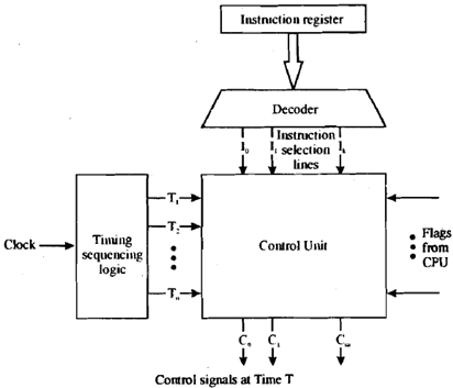
The other method is hard-wired control, which is usually the preferred approach for RISC architectures like MIPS and RISC-V. Hard-wired control uses “AND”, “OR”, and “NOT” gates (along with the various components we’ve learned can be built from these gates, like MUXes and DEMUXes) to produce the appropriate control signals. The instruction decoder takes in an instruction and outputs all of the control signals for that instruction.
The method you choose to implement your control unit is one of the major design decisions you get to make in this project; we recommend the hard-wired control option because it is more realistic, but past students have been successful with both approaches.
(4) Pipelining
Your processor will have a 2-stage pipeline:
1. Instruction Fetch: An instruction is fetched from the instruction memory. (Note: while you can, please do not calculate jump address in this stage. Instead, you should try to deal with the jump control hazard.)
2. Execute: The instruction is decoded, executed, and committed (written back). This is a combination of the remaining stages of a normal five-stage RISC-V pipeline.
First, make sure you understand what hazards you will have to deal with.
The instruction immediately after a branch or jump is not executed if a branch is taken. This makes your task a bit more complex. By the time you have figured out that a branch or jump is in the execute stage, you have already accessed the instruction memory and pulled out (possibly) the wrong instruction. You will therefore need to “kill” instruction that is being fetched if the instruction under execution is a jump or a taken branch. Instruction kills for this project MUST be accomplished by MUXing a nop into the instruction stream and sending the nop into the Execute stage instead of using the fetched instruction. 0x00000013, or addi x0, x0, 0 is a nop instruction, as it has no effect on the state of the processor.
You should only kill if a branch is taken (do not kill otherwise). Do kill on every type of jump. Do not solve this issue by calculating branch offsets in the IF stage. Because we test your output against the reference every cycle, and the reference returns a nop, while it may be a conceptually correct solution, this will cause you to fail our tests.
Because all of the control and execution is handled in the Execute stage, your processor should be more or less indistinguishable from a single-cycle implementation, barring the one-cycle startup latency and the branch/jump delays. However, we will be enforcing the two-stage pipeline design. Some things to consider:
- Will the IF and EX stages have the same or different
PCvalues? - Do you need to store the
PCbetween the pipelining stages? - To MUX a
nopinto the instruction stream, do you place it before or after the instruction register? - What address should be requested next while the EX stage executes a
nop? Is this different than normal?
As an example of what pipelining behavior should look like, consider this simple assembly program:
    add t0, t0, t2
    jal ra label
    sub t0, t2, t2
    div t1, t0, t2
label: mul t0, t0, t0
    xor t0, t1, t2
    ...
The instructions would proceed through the two stages of the datapath (IF and EX) as follows:
| Clock Cycle | Instruction Fetch (IF) | Execute |
| 1 | add | nop |
| 2 | jal | add |
| 3 | sub | jal |
| 4 | mul | nop |
| 5 | xor | mul |
| 6 | ... | xor |
Notice what happens in both stages, particularly in cycles 3 and 4–where does the nop enter the instruction stream? What happens to the sub instruction?
You might also notice a bootstrapping problem here: during the first cycle, the instruction register sitting between the pipeline stages won’t contain an instruction loaded from memory. What will send a nop into the EX stage for the first cycle–how do we deal with this? It happens to be the case that Logisim automatically sets registers to zero on reset. In RISC-V, this instruction (all 0’s) actually corresponds to one of the compressed instructions, which we will not implement in this project. You can treat the instructiom, 0x00000000, as a nop; we’d just like you to be aware that this is a small deviation from real RISC-V.
Remember that if you’d like to reset your processor, go to simulate --> Reset Simulation (Ctrl+R).
Getting Started: A Guide
We know that trying to build a CPU with a blank slate might be intimidating, so we want to guide you through how to think about this project by implementing a simple I-type instruction, addi.
Recall the five stages of the CPU pipeline:
- Instruction Fetch
- Instruction Decode
- Execute
- Memory
- Write Back
This guide will help you work through each of these stages, as it pertains to the add instruction. Each section will contain questions for you to think through and pointers to important details, but it won’t tell you exactly how to implement the instruction.
You may need to read and understand each question before going to the next one, and you can see the answers by clicking on the question. During your implementation, feel free to place things in subcircuits as you see fit.
Stage 1: Instruction Fetch
The main thing we are concerned about in this stage is: how do we get the current instruction? From lecture, we know that instructions are stored in the instruction memory, and each of these instructions can be accessed through an address.
(1) Which file in the project holds your instruction memory? How does it connect to your cpu.circ file?
The instruction memory is the ROM module in `run.circ`. It provides an input into your CPU named "Instruction" and takes an output from your CPU named "fetch_addr".(2) In your CPU, how would changing the address you output to fetch_addr affect the instruction input?
The instruction that `run.circ` outputs to your CPU should be the instruction at address `fetch_addr` in instruction memory.(3) How do you know what the fetch_addr should be? (Hint: it is also known as PC)
`fetch_addr` is the address of the current instruction being executed, so it is saved in the PC register. For this project, it's fine for the PC to start at 0, and that is the default value for registers.(4) For basic programs without any jumps or branches, how will the PC change from line to line?
The PC must increment by 1 instruction in order to go to the next instruction, as the address held by the PC register represents what instruction to execute. By default, we increment the PC by 4, as we assume it is a byte address.We have provided the PC register in the cpu.circ file. Please implement the PC’s behavior for simple programs - ignoring jumps and branches. You will have to add in the latter two in the project, but for now we are only concerned with being able to run strings of addi instructions. Where should the output of the PC register go? Remember to connect the clock! Remember that we’re implementing a 2-stage pipelined processor, so the IF stage is separate from the remaining stages. What circuitry separates the different stages of a pipeline? Do you need to add anything?
Stage 2: Instruction Decode
Now that we have our instruction coming from the instruction input, we have break it down in the Instruction Decode step, according to the RISC-V instruction formats you have learned.
(1) What type of instruction is addi? What are the different bit fields and which bits are needed for each?
I type. The fields are: - imm [31-20] - rs1 [19-15] - funct3 [14-12] - rd [11-7] - opcode [6-0](2) In Logisim, what tool would you use to split out different groups of bits?
Splitter!(3) Implement the instruction field decode stage using the instruction input. You should use tunnels to label and group the bits.
(4) Now we need to get the data from the corresponding registers, using the register file. Which instruction fields should be connected to the register file? Which inputs of the register file should it connect to?
Instruction field `rs1` will need to connect to read register 1.(5) Implement reading from the register file. You will have to bring in your RegFile from Project 3-1. Remember to connect the clock!
(6) What does the Immediate Generator need to do?
For addi, the immediate generator takes in 12 bits and produces a signed 32-bit immediate. We highly suggest you create an Immediate Generator subcircuit!Stage 3: Execute
The Execute stage, also known as the ALU stage, is where the computation of most instructions is performed. This is also where we will introduce the idea of using a Control Module.
(1) For the addi instruction, what should be your inputs in to the ALU?
Read Data 1 and the immediate produced by the Immediate Generator.(2) In the ALU, what is the purpose of ALU_Sel?
It chooses which operation the ALU should perform.(3) Although it is possible for now to just put a constant as the ALUSel, why would this be infeasible as you need to implement more instructions?
With more instructions, the input to the ALU might need to change, so you would need to have some sort of circuit that changes ALUSel depending on the instruction being executed.(4) Create a new subcircuit for the Control Module. This module will need to take in as inputs the opcode, funct3, and funct7, and (for now) use these to output a value for ALUSel, depending on what the current instruction is. Read over the “Control” section above for some suggestions about different approaches for doing this. As you implement more instructions, this circuit will have to expand and become more complex.
(5) Bring in your ALU and connect the ALU inputs correctly. Do you need to connect the clock? Why or why not?
Stage 4: Memory
The memory stage is where the memory can be written to using store instructions and read from using load instructions. Because the addi instruction does not use memory, we will not spend too much time here.
Bring in the MEM module that we provided. At this point, we cannot connect most of the inputs, as we don’t know where they should come from. However, you can still connect the clock.
Stage 5: Writeback
The write back stage is where the results of the operation is saved back to the registers. Although not all instructions will write back to the register file (can you think of some which do not?), the addi instruction does.
(1) Looking at the entire ISA, what are some of the instructions that will write back to a register? Where in the datapath would it get the values?
`addi` is an example that will take the output from the ALU and write it back. `lhu` will take the output from MEM and write it to a register.(2) Let’s create the write back phase so that it is able to write both ALU and MEM outputs to the Register File. Later, when you implement branching/jumping, you may need to add more to this mux. However, at the moment, we need to choose between the ALU and MEM outputs, as only one wire can end up being an input to the register file. Bring a wire from both the ALU and MEM, and connect it to a MUX.
(3) What should you use as the Select input to the MUX? What does the input depend on?
This input should be able to choose between the two MUX inputs, ALU and MEM, which means that its value depends on which instruction is executing. This suggests that the input should originate from the Control Module, as the Control Module is responsible for figuring out which instruction is executing. We'll need another control signal here, commonly called WBSel. WBSel determines which value to write back to the RegFile.(4) Now that we have the inputs to the MUX sorted out, we need to wire the output. Where should the output connect to?
Because the output is the data that you want to write into the Register File, it should connect to the Write Data input on the Register File.(5) There are two more inputs on the Register File which are important for writing data: RegWEn and rd. One of these will come from the Instruction Decode stage and the other one will be a new control signal that you need to design. Please finish off the Writeback stage by these inputs on the RegFile correctly.
If you have done all of the following steps correctly, you should have a processor that works for addi instructions. You can run ./cpu-sanity.sh and see if it’s working correctly! You should pass the first test: CPU-addi. For the rest of the project, you will be implementing more instructions in much the same way–connecting outputs to inputs, adding MUXes and other Logisim components, and defining new control signals. Hopefully, this will be an easier task now that you have a basic skeleton to work off of. Good luck!
Testing
Part of your grade for Project 3-2 will be writing a suite of tests for your project, which we will assess for coverage, so please read this entire section of the spec carefully, and ask questions on Piazza if you’re confused!
Understanding how the tests work
Each test is a copy of the run.circ file included with the starter code that has instructions loaded into its IMEM. When you run logisim-evolution from the command line, the clock ticks, the program counter is incremented, and the values in each of the outputs is printed to stdout.
Let’s take as an example one of the 4 sanity tests included with the starter code, CPU_addi.circ. This is a very simple test that has 3 addi instructions (addi t0, x0, 5, addi t1, t0, 7, addi s0, t0, 9), meant for a first sanity check after you go through the “Getting Started” guidelines above.
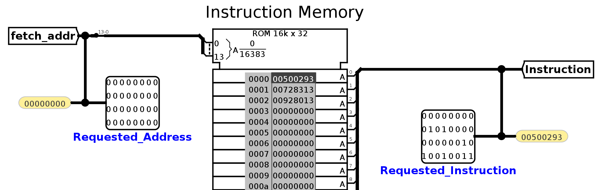
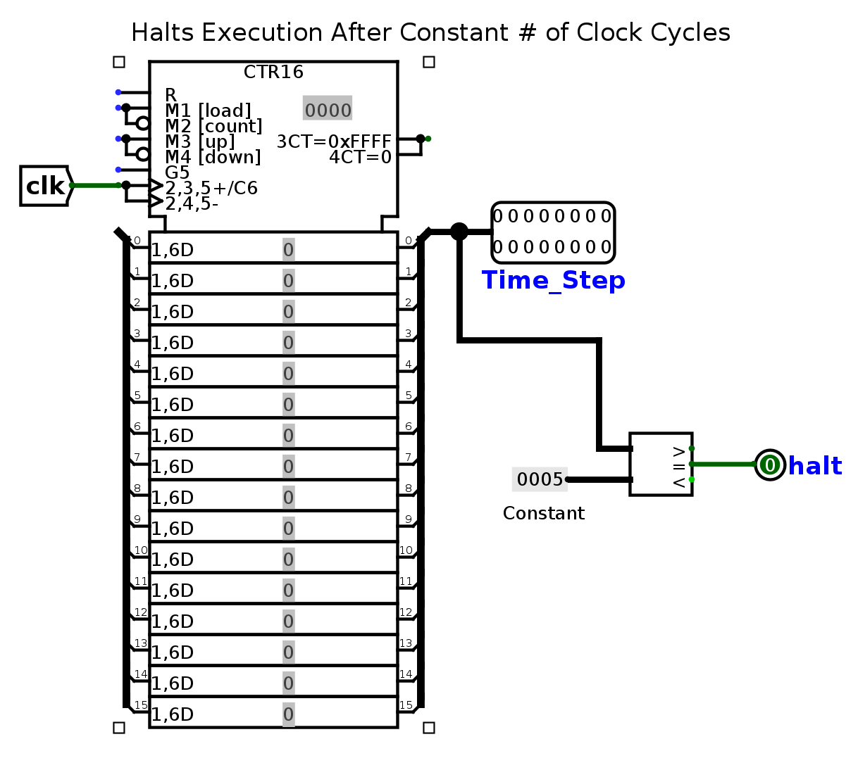
If you open CPU_addi.circ in Logisim Evolution, it’ll look like this:
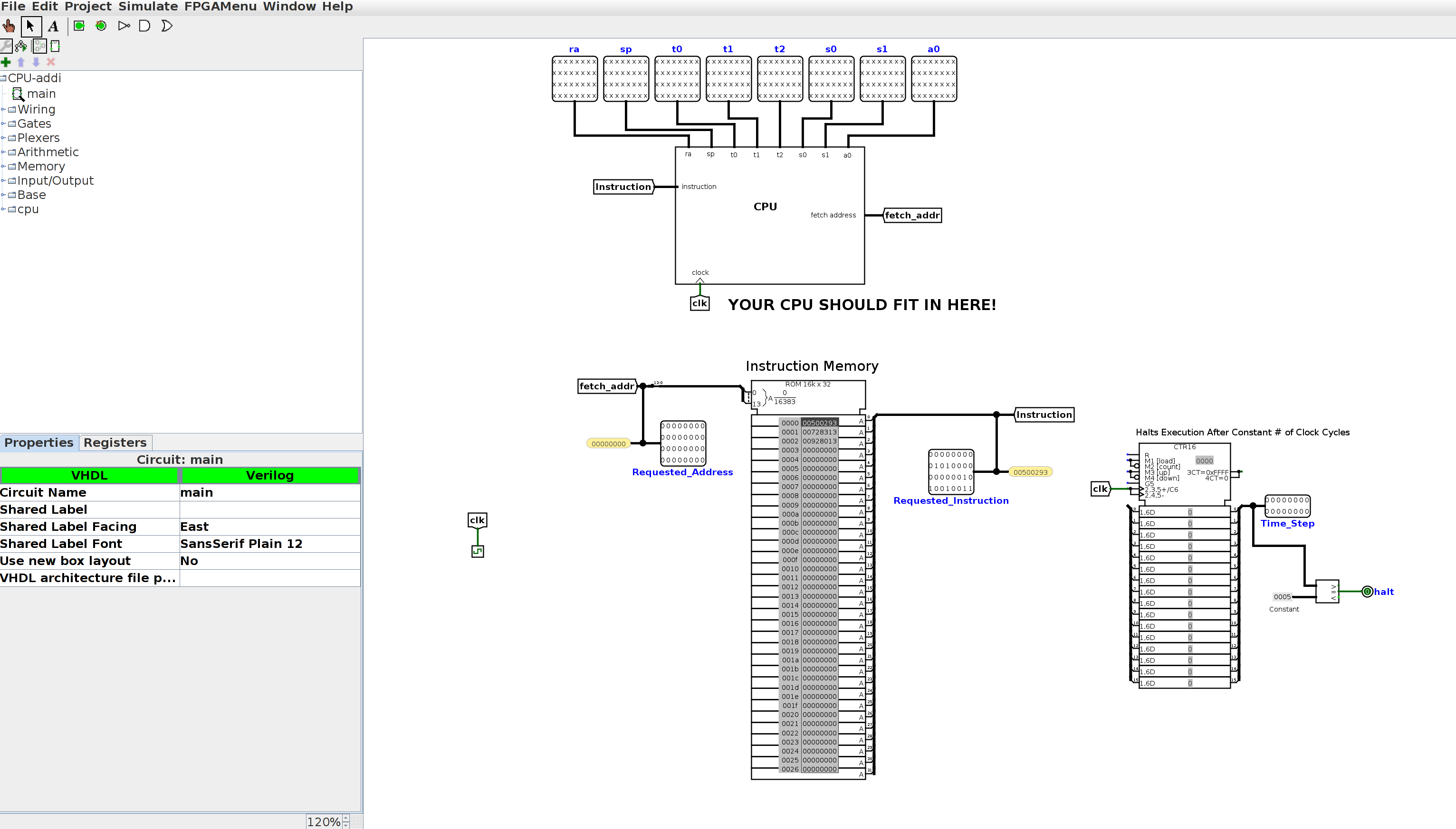
Let’s take a closer look at the various parts of the test file. At the top, you’ll see the place where your CPU is connected to the test outputs. With the skeleton file, you’ll see all xxxx’s, as you do below; when your CPU is working, this should not be the case. Your CPU takes in one input (instruction), and along with the values in each of the registers, it has one additional output: fetch_addr, or the address of the instruction to be fetched from IMEM to be executed the next clock cycle.
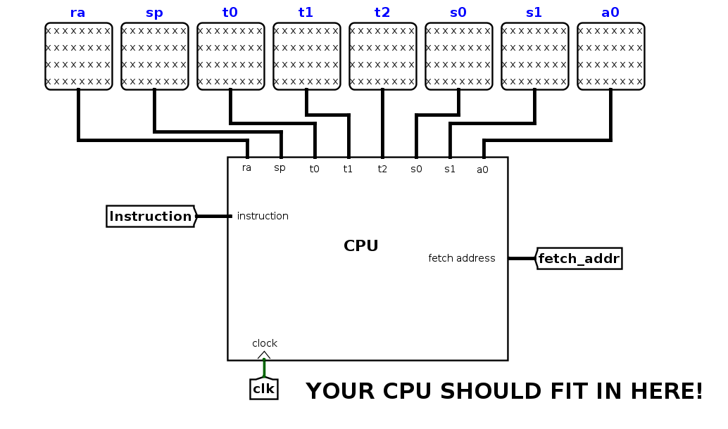
Be careful that you don’t move any of the inputs/outputs of your CPU around, or add any additional inputs/outputs. This will change the shape of the CPU subcircuit, and as a result the connections in the test files may no longer work properly.
Below the CPU, you’ll see instruction memory. The hex for the 3 addi instructions (0x00500293, 0x00728313, 0x00928413) has been loaded into instruction memory. Instruction memory takes in one input (called fetch_addr) and outputs the instruction at that address. fetch_addr is a 32-bit value, but because Logisim Evolution caps the size of ROM units at 2^16B, we have to use a splitter to get only the bottom 14 bits of fetch_addr. Notice that fetch_addr is a word address, not a byte address.
So what happens when the clock ticks? Each tick of the clock increments an input in the test file called Time_Step. The clock will continue to tick until Time_Step is equal to the halting constant for that test file (for this particular test file, the halting constant is 5). At that point, the Logisim Evolution command line will print the values in each of your outputs to stdout. Our tests will compare this output to the expected; if your output is different, you will fail the test.
Sanity Tests
We’ve included 6 sanity tests for you with the starter code. You can run them using ./cpu-sanity.sh.
Six sanity tests have been included for you with the starter code: CPU-addi.circ, CPU-add_lui_sll.circ, CPU-mem.circ, CPU-branch.circ, CPU-br_jalr.circ, and CPU-jump.circ. You can see the .s files and hex corresponding to each of these tests in the tests/input directory. Run them using the following command from your main Project 3-2 directory:
./cpu-sanity.sh
Like in Project 3-1, we’ve included a Python script to make it a bit easier to interpret your test output. It’s called binary_to_hex.py. It is in the tests/circ_files directory. You can run it on the reference output for CPU-addi.circ with the following command:
python binary_to_hex.py reference_output/CPU-addi.out
or, on your CPU’s output with the following command:
python binary_to_hex.py output/CPU-addi.out
Writing your own tests
The autograder tests fall into 3 main categories: unit tests, integration tests, and edge case tests. We won’t be revealing to you what these tests are specificaly, but you should be able to re-create a very close approximation of them on your own in order to test your datapath.
What is a unit test? A unit test exercises your datapath with a single instruction, to make sure that each individual instruction has been implemented and is working as expected. You should write a different unit test for every single instruction that you need to implement, and make sure that you test the spectrum of possibilities for that instruction thoroughly. For example, a unit test slt should contain a case both where rs1 < rs2 and where rs1 !< rs2.
Part of your submission for this project will be a unit test suite, and part of your grade will be unit test coverage. In one or more .s files, you will submit your unit test suite to the Project 3-2 Test Coverage autograder, and you will receive an assessment of the completeness of your unit tests. The tests themselves will be 5 percent of your grade, and unit tests are 20 percent of your grade, so don’t take this lightly!
What is an integration test? After you’ve passed your unit tests, move onto tests that use multiple functions in combination. Try out various simple RISC-V programs that run a single function; your CPU should be able to handle them, if working properly. Feel free to use riscv-gcc to compile C programs to RISC-V, but be aware of the limited instruction set we’re working with (you don’t have any ecall instructions, for example).
Finally, edge cases! What edge cases should you look for? A hint from us: our 2 main classes of edge cases come from memory operations and branch/jump operations (we call them something along the lines of “mem-full” and “br-jump-edge”). Think about all the different ways these operations could go wrong.
You can optionally submit your integration and edge case tests to the test coverage autograder. We will give you an integration/edge case test coverage estimate; this will not be graded but will give you a method of assessing whether or not you should be looking for more edge cases to test.
Creating your tests
For this project, we will not be releasing all the tests. However, we have included some scripts to make test creation a little bit easier on you. Included in the starter code is a file called create_test.py. It expects 1 argument: .s files containing the RISC-V code you wish to test. The script will then generate copies of run.circ with your new tests loaded in for you, along with some other files. For everything to work properly:
- Write your tests and name them whatever you would like, but be sure to save them as .s files
- Don’t move the tests anywhere, keep them (as well as
create_test.py) in the root directory of the project -
Run:
python create_test.py <test 1 name here>.s <test 2 name here>.s ...
Your file hierarchy should now contain some new things:
fa18-proj3-2-starter
        -- <test name here>.s  # Your test
        -- my_tests
          -- circ_files
            -- cpu.circ, mem.circ  # Your circuits
            -- output
            -- reference_output
            -- CPU-<test name here>.circ  # The new circuit containing your test
         -- input
            -- <test name here>.hex  # The hex dissasembly of your test
            -- <test name here>.s  # A copy of your test
Now that everything is created, to test your own tests, run:
./cpu-user.sh
If you wish to delve into your the circuit running your test, you can simulate it by opening up the CPU-<test name here>.circ file. If you don’t remember how to simulate your circuit, please refer back to the Logism labs. We highly encourage you to poke your circuit while the test is running to observe how your circuit reacts to various inputs (perhaps this can give you ideas for new tests to write).
If you wish to simulate your code only for a certain number of cycles, you can do that by running the following:
python create_test.py <test name here>.s -n <number of cycles>
If you would like to decode your output, use the provided binary_to_hex.py on the appropriate .out file in the output folder shown above. Be aware that because you’re implementing a 2-stage pipelined processor and the first instruction writes on the rising edge of the second clock cycle, the effects of your instructions will have a 2 instruction delay. For example, let’s say I have written a test with one instruction:
addi t0, x0, 1
The output will actually come out to be:

Note how t0 doesn’t get changed until line 3. NOTE: This testing harness assumes you have the 2-stage pipeline implemented. You should first concern yourself with getting the single-cycle working, then the 2-stage, then the sanity tests, and then your own tests. The sanity tests do NOT test every instruction mentioned in the spec, so make sure you are writing extra tests!
Our testing apparatus is a fairly new innovation, though we (and a semester’s worth of previous students) have tested it fairly thoroughly. However, if you notice any behavior you believe might be a bug, please let us know on Piazza!
Using Web Venus
Although we have specified three custom additional instructions, Venus does not support them because they are not standard or standard extension instructions. Because of this, one of your TA’s Stephan (the person maintaining Venus), made a package system with which you can make custom packages for Venus. There is a package which will add the lwc, pop, and push instructions to Venus so that you can properly test these custom instructions with the web version of Venus!
Here is how you would go about doing this: Either 1) click on this link which should auto add the package (https://venus.cs61c.org?packages=https://cs61c.org/sp19/projects/proj3/proj3_2-venus_package.js) or 2) go to https://venus.cs61c.org. Click on the Venus tab at the top (it is the left most one). Now look for the settings secetion (it should be on the right if your screen is large enough otherwise you will have to scroll down to see it). From there you should click on the Packages word to see the packages which you can enable/disable or add or remove. Next paste this link (https://cs61c.org/sp19/projects/proj3/proj3_2-venus_package.js) in the box and then click add package. You should see a message saying Loaded script (https://cs61c.org/sp19/projects/proj3/proj3_2-venus_package.js)! Now you can actually use the custom instructions in the web version of Venus just as if they were normal instructions! (This is still very experimental as Stephan really just implemented some of these features recently, so please report any bugs you may find on Piazza).
Grading and Submission
Grading
20% of Project 3 was Project 3-1, the RegFile and ALU. There was a potential for 3% extra credit if you implemented signed mulh properly. The remaining 80% comes from Project 3-2. Of this 80%, 5% comes from your unit test coverage score, and the remaining 75% comes from autograder tests. Unlike Project 3-1, we will not be releasing all of the tests. The grading breakdown of the 75 points for autograder tests is as follows: 20 points for Unit Tests, 20 points (3-4 points each) for the provided Sanity Tests, and 35 points for edge case/integration tests. When you submit to the project autograder on Gradescope, you will see your results for the Sanity Tests, but not for the remaining tests; we will release your full scores after the deadline.
For test coverage, submit to the “Project 3-2: Test Coverage” autograder on Gradescope.
We’re still working out a couple kinks in the autograders, but both will be available well before the project deadline. If you submit to either the CPU or the test coverage autograder before the autograder is available, an e-mail will be sent to you once your submission is processed and scored. We will also make a Piazza announcement when they go up.
Submission
Your final submission for this project will be on Gradescope, in two parts: your CPU and your tests. The name of the assignments are “Project 3-2: CPU” and “Project 3-2: Test Coverage”.
For “Project 3-2: CPU”, you have two options for which files to submit. If you’ve made some changes to your Project 3-1 RegFile and ALU that your solution for Project 3-2 is dependent on, please upload your alu.circ and regfile.circ files along with your cpu.circ file. Otherwise, simply upload your cpu.circ file and we will run the autograder tests on it with our staff solution for the ALU and RegFile.
For “Project 3-2: Test Coverage”, zip your entire part2 directory and submit it; if you have been following the directions above, you should have been creating your .s files in your part2 directory.