 and
and  for the transmitter on
one side, and
for the transmitter on
one side, and  with the same
  for the
transmitter on the other side. This permits full duplex communication.
for the
transmitter on the other side. This permits full duplex communication.
EECS20: Introduction to Real-Time Digital Systems
Lab12: BFSK Modem
EECS20: Introduction to Real-Time Digital Systems
©1996 Regents of the University of California.
By K. H. Chiang, William T. Huang, Brian L. Evans.
URL: http://www-inst.eecs.berkeley.edu/~ee20
News: ucb.class.ee20
In this lab, we will implement a BFSK (Binary Frequency Shift Keying) modem on the C50 DSK. The background sections provides you with some theories behind practical FSK implementations while we are goind to implement a simple yet impractical scheme. The scheme likens the DTMF scheme reviewed here in the DTMF Example section. In the writeup, you will write a C50 code to decode a very slow BFSK modem waveform.
 to represent a binary 0, and
  to represent
a binary 1. Note that is typically chosen such that
to represent
a binary 1. Note that is typically chosen such that  .
.
To put some numbers into this, 300 bps connections use FSK with
and for the transmitter on
one side, and with the same for the
transmitter on the other side. This permits full duplex communication.
The typical transmitter setup appears as in Figure 1.
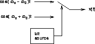
Figure 1: FSK transmitter.
We choose what cosine to send based on the current bit. If the current bit is
0, we send , and if the current bit is 1, we send
.
What do we do at the receiver? One thing we could try is to arrange for two
bandpass filters, one passing frequencies centered about  and the
other passing frequencies centered about
and the
other passing frequencies centered about  , as in
Figure 2.
, as in
Figure 2.
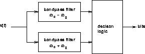
Figure 2: FSK receiver using bandpass filters.
If we then look at the outputs of the two filters, we can make a decision about what bit is currently being received, depending on the amplitude of the output of the two filters.
As illustrated in Figure 3,
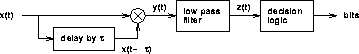
Figure 3: FSK receiver using a multiplier and a delay.
another thing to try would be to take the received signal  and multiply
it by a delayed version of the received signal
and multiply
it by a delayed version of the received signal  . We can then
bandpass the output of the multiplier to obtain a low frequency content signal
whose sign indicates what bit was received. This assumes the correct choice of
the delay
. We can then
bandpass the output of the multiplier to obtain a low frequency content signal
whose sign indicates what bit was received. This assumes the correct choice of
the delay  and the low pass filter cutoff frequency.
Let's examine this in greater detail. Assume that 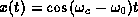 is
being received. If we multiply this by a delayed version of itself, we end up
with:
is
being received. If we multiply this by a delayed version of itself, we end up
with:
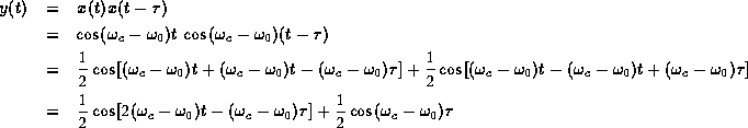
If we pass this through a low pass filter that has a cutoff frequency
 , we end up with the second term. The filter output
 is then:
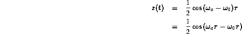
If we choose to be such that  , then
 and further reduces to:
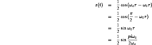
Since :
which is positive.
A similar argument can be made for receiving ; is
then found to be negative.
So from the sign of we can figure out what was actually sent. If
is positive, then a binary 0 was sent, and if is negative, then a binary
1 was sent.
We can treat a DTMF as a variation of the FSK. Since we are not going to address the issue of synchronizing the transmitter and receiver, we will parse the bits with pause as we did in the DTMF codec.
Please study the following two C50 assembly files for DTMF waveform
generation and decoding. They will help you to write the C50 code
for a simpler Binary FSK decoder. The DTMF generationg code
gentt.asm is provided to you
so you can test the decoder. It repeats a sequence of waveform
for a sequence of digits. The DTMF decoder code
decode.asm passes the input waveform through filter
banks, calculate the energy in each band and makes decision on which
digit has been transmitted. You may not be able to understand the
Calculation of the Goertzel filter output and its Energy,
but the implementation of the decision logic should give you some
insight on the touch tone protocol and the parsing of digits or bits
through pauses. To assemble the decoder you need the file
template.asm in the same
directory. You are encouraged to use the template file to initiate
of the DSK after examinng the file to avoid address conflicts.
Note: The output of this DTMF decoder is a sequence of hex numbers representing the telephone key pad according to the following table. The output is stored in a circular buffer in the DSK data memory from address 1000h to 1FFFh.
In your writeup, concisely record your modification to the code and comment the code you write carefully.
You should read about the C50 instructions: BANZ,
MADD, MADS, and SPH before you proceed.
bfskgen.asm to find
out the two frequencies used to represent 0 and 1. Alternatively,
you can write your own waveform generation code and specify
your own frequencies. You should also find out the duration
of the pulses and pauses.
hp10.asm.
This filter interfaces directly with the RCA jacks. You can
connect the output to speaker and the input to any waveform
sources. Does it work on the electronic keyboard? Does it
work on the BFSK waveform generator?
dpow.asm to store the
pair (high pass and low pass) of sequences of calculated
energy in the data memory. Make sure you can decode the
transmitted bit sequences by inspecting the stored values.
ACC	Accumulator register that stores intermediate results
ADD	Add to ACC, a C50 instruction
ADDB	Add ACCB to ACC, a C50 instruction
AIC	Analog Interface Circuit that allows analog devices to be connected to the C50 DSK board
ALU	Arithmetic Logic Unit that adds, shifts, and performs logical operations.
APAC	Add PREG to ACC, a C50 instruction
AR	Auxiliary register that stores indirect pointer to addresses
ARn	Auxiliary register number n(0-7)
ARP	Auxiliary register pointer that points to currently used AR
B	Branch Unconditionally, a C50 instruction
BCND	Branch Conditionally, a C50 instruction
C50	Texas Instruments TMS 320C50 DSP processor (16-bit, 28.6/20 MIPS)
CALL	Call Unconditionally, a C50 instruction
CBCR	Circular buffer control register that selects ARn and enable/disable the buffers n(1,2)
CBERn	Circular buffer end register that stores the last address in the circular buffer n(1,2)
CBSRn	Circular buffer start register that stores the first address in the circular buffer
CLRC	Clear Control Bit, a C50 instruction
DMOV	Data Move in Data Memory, a C50 instruction
DP	Data memory page pointer that points to the current 128-byte page of data memory
DSK	DSP Starter Kit, a C50 development package
DSP	Digital Signal Processor, a special-purpose microprocessor
DXR	Data transmit register that stores samples to be transmitted to AIC
EXAR	Exchange ACCB with ACC, a C50 instruction
INDX	Index register for indirect addressing
LACC	Load ACC, a C50 instruction
LACL	Load Low ACC and Clear High ACC, a C50 instruction
LAMM	Load ACC with Memory-Mapped Register, a C50 instruction
LAR	Load ARn, a C50 instruction
MACD	Multiply and Accumulate with Data Move, a C50 instruction
MADD	Multiply and ACC with Data Move and Dynamic Addressing, a C50 instruction
MAR	Modify ARn and ARP, a C50 instruction
NEG	Negate ACC, a C50 instruction
PLU	Parallel logic unit that performs logical operations in parallel to ALU
PREG	Product register that stores multiplication results
RET	Return From Subroutine, a C50 instruction
RETE	Return From Interrupt, a C50 instruction
RCA	A connector standard
SACH	Shift Accumulator and Store High Word Result, a C50 instruction
SACL	Shift Accumulator and Store Low Word Result, a C50 instruction
SAMM	Store ACC to memory-mapped register, a C50 instruction
SPLK	Store long immediate to data memory location, a C50 instruction
ZAC	Zero ACC, a C50 instruction
ZAP	Zero ACC and PREG, a C50 instruction