Digital Circuit Design: Problem
Circuit topology
Design variables
Design objective
Circuit Topology
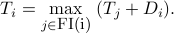
The combinational circuit consists of  connected gates, with primary inputs and outputs. We assume that there are no loops in the corresponding graph. For each gate, we can define the fan-in, or set of predecessors of the gate in the circuit graph, and the fan-out, which is its set of successors.
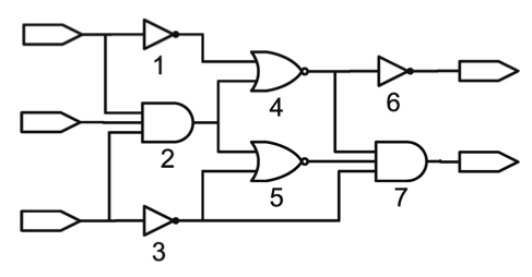 |
Circuit topology: A digital circuit that consists of several ‘‘gates’’ (logical blocks with a few inputs and one output) connecting primary inputs, labeled 
By definition, the primary inputs have empty fan-in, and the primary outputs have empty fan-out. |
 , to primary outputs, labeled
  . Each gate is represented by a symbol that specifies its type; for example, the gates labelled
  and
and  are inverters. For this circuit, the fan-in and fan-out of gate
  is
isDesign Variables
The design variables in our models are the scale factors, which we denote by  ,
,  , which roughly determine the size of each gate. These scale factors satisfy
  , , where
  corresponds to a minimum-sized gate, while a scale factor
  corresponds to the case when all the devices in the gate have
  times the widths of those in the minimum-sized gate.
The scale factors determine the size, and various electrical characteristics, such as resistance and conductance, of the gates. These relationship can be well approximated as follows:
The area of gate
 is proportional to the scale factor :
  , with
  . (So, you can simply think of the scale factors as the areas.)
The intrinsic capacitance of gate
is of the form
with  positive coefficients.
The load capacitance of gate
is a linear function of the scale factors of the gates in the fan-out of gate :
where  are positive coefficients.
Each gate has a resistance that is inversely proportional to the scale factor (the larger the gate, the more current can pass through it):
with  positive coefficients.
The gate delay is a measure of how fast the gate implements the logical operation it is supposed to perform; this delay can be approximated as

We observe that all the above parameters are actually posynomials in the (positive) design vector  .
.
Design Objective
A possible design objective is to minimize the total delay  for the circuit. We can express the total delay as

where  represents the latest time at which the output of gate can transition, assuming that the primary inputs signals transition at
  . (That is, is the maximum delay over all paths that start at primary input and end at gate .) We can express via the recursion
The operations involved in the computation of involve only addition and point-wise maximum. Since each  is a posynomial in , we can express the total delay as a generalized posynomial in .
|
|
Recursion for the total delay: For the circuit on the left, the total delay 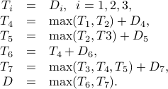
|